Chinese semiconductor thread II

gelgoog

Lieutenant General
Registered Member
The information in it is very inconsistent.
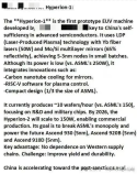
It says they are trailing it in SMIC Beijing 200mm fab to verify 5nm node. All SMIC Beijing fabs are 300mm and mature node. If they are verifying 5nm node, most ideal location is Shanghai.
SMIC Beijing, the latest fab, has lots of empty space to add whichever tools are necessary. And a 200mm production line would need less light source power to reach a given productivity in wafers per hour. So who knows.

It also claims SMEE is trying LPP route. But from everything we have seen here before, SMEE is not involved in EUV litho, perhaps other than the MET we saw earlier.
Then it says v1 throughput is 10 WPH and v2 throughput will be 150 WPH. Then in the next paragraph it says it can process 250 wafers per hour surpassing ASML's 190 (which is not accurate either).
I remember ASML's early EUV prototypes also had horrible WPH productivity because the light source was too weak. But it allows you to prototype processes and materials.
 

huemens

Junior Member
Registered Member
SMIC Beijing, the latest fab, has lots of empty space to add whichever tools are necessary. And a 200mm production line would need less light source power to reach a given productivity in wafers per hour. So who knows.


I remember ASML's early EUV prototypes also had horrible WPH productivity because the light source was too weak. But it allows you to prototype processes and materials.

This is a version of it I saw about 2 months ago on Twitter. Obviously this rumor has evolved since then.

euv__1.png
 
Last edited:

tokenanalyst

Lieutenant General
Registered Member
Yes, But all their Bejing fabs are 300mm. 200mm fabs are in other cities.

And this post started appearing in social media several months ago. At that time it did not have the above things I mentioned, so most likely people just made up and added things on their own as they went on passing the rumor.
These tools are not send to the SMIC fabs, directly, but pilot lines. Sending this tool to a SMIC fab I think will disrupt production.

As I said, China innovation centers (looks like there is a number of them) in this case for advanced sensors, are building purely domestics pilot lines all over China, this basically acts as places for China to develop new technologies like GAAFET or in this case, advanced sensors. CIS imaging, MEMs and so on. But also act as a platform for the verification of domestics tools in real production. My guess that companies test/produce products in these centers and then copy-scale exact for commercialization with same or similar domestic tools. Quite interesting.

These production lines also may act as mass production centers for state institutions and companies. They could get technologies that doesn't exist in the market.

View attachment 160603
Advanced EUV Pilot lines for EUV Metal Organic Photoresist.

According to the Wuxi government website, the 2025 Integrated Circuit (Wuxi) Innovation and Development Conference opened on September 4.

Several major projects were announced at this conference. In addition to the computing power platform, there are two other projects worth noting - the Wuxi Advanced Process Semiconductor Nanoscale Photoresist Pilot Line is the first innovative platform in the country to master the core raw materials, formulas and application technologies of MOR-type photoresist. The photoresist it develops and produces will be world-class.

The other is the Jiangsu (Jicui) Photoresist Resin Synthesis Pilot Line, which is the only R&D platform in the country that uses continuous flow technology to prepare photoresist resins. It is the first polymerization equipment and process for the stable synthesis of polymers.

Among them, MOR photoresist is a new technology for photoresist in the EUV era. It refers to metal oxide photoresist, which replaces the CAR chemical amplification photoresist currently used in DUV photoresist. It is one of the key materials for improving photolithography resolution, reducing gate pitch, and reducing defect rate.​
EUVL Technologies Research (started in 2000) -> EUV Prototypes (2017) -> EUV Pilot Lines(2022-2023?) -> Commercialization and Risk Production (2027-2028?)
 

jx191

New Member
Registered Member
A pilot line is step way beyond the lab and a step closer to mass production.
But do we know that pilot lines are definitely up and running? Rumours are common, and we can use the patents and R&D reports, but I haven't heard anything concrete about pilot lines for EUV yet.
 

ENTED64

Junior Member
Registered Member
But do we know that pilot lines are definitely up and running? Rumours are common, and we can use the patents and R&D reports, but I haven't heard anything concrete about pilot lines for EUV yet.
We don't know anything concrete and probably won't in the near future. Fact is for some years now rumors/patents/reports have basically been all we've got because of increased OPSEC, especially for EUV. So if you're looking for something like a formal announcement from the company that this pilot line is up and running, you're not going to get it even if it is up and running.
 

tokenanalyst

Lieutenant General
Registered Member
But do we know that pilot lines are definitely up and running?
For EUV? I Do think from quite some time. Immersion and EUV where two projects going hand to hand. Immersion is probably in a more advanced stage than EUV, 14 nm this year according to sources. Given that Immersion and dry lithography are more closely related than immersion and EUV.

Rumours are common, and we can use the patents and R&D reports, but I haven't heard anything concrete about pilot lines for EUV yet.
They are not going to shout it or there is a lot of secrecy on the matter. They are developing a lot of EUVL tech that goes way beyond lab experiments and more for a EUVL ecosystem.
 
Top