Chinese semiconductor thread II

sunnymaxi

Major
Registered Member
I find that highly unlikely, as SMEE is a company under the Shanghai SASAC, while Yuliangsheng is under the Shenzhen SASAC.
If you understand China, you'd know that for the sake of their own performance records, two SASACs would never hand such a prime project over to their rival. Unless the State Council steps in to mediate.
yes. this is unlikely. this is mostly Joint veture.

SMEE is a flagship project of Shanghai SASAC.. and SMEE has big plans in near future.
 

snake070

New Member
Registered Member
Do you know what each one have, when they started being used for production and how they compare or correspond to which of ASML's and Nikon's DUV machines
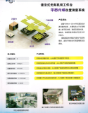
This topic could fill an entire thesis. I recall Havok mentioning in late 2022 that certain piping components within lithography machines were sourced from Japan. So the 85% localization rate isn't a recent milestone.
The first-generation 28nm lithography machine utilized a laser interferometer.
The second-generation 28nm lithography machine employed a planar grating interferometer. Its overlay accuracy supports 10nm processes, equivalent to TSMC's 7nm node.
As for current progress, secrecy levels are extremely high now, with fake news everywhere, making it hard to predict.
The English edition of the Financial Times has considerable accuracy, having reported as early as 2019 on Huawei establishing domestic production lines at ICRD. So keeping an eye on the Financial Times is advisable. Domestically, focus mainly on academic papers—too much of the news is fake.

Uprecision.png
 

sunnymaxi

Major
Registered Member
How far in the pipeline are the machines equivalent to the 2050i, 2100i, and 2150i or even better than the 2150i?
its successor already does exist and called ''SSA900i''.. an improved version of SSA800i.. there are plenty of information available on semiconductor older thread. which is closed now. but anyone can visit and read.
 
  • Like
Reactions: zbb

tphuang

General
Staff member
Super Moderator
VIP Professional
Registered Member
It’s interesting that this report phrases its snippet on EUV as “SiCarrier is pursuing an EUV lithography project” and doesn’t make mention of any other efforts outside the context of SiCarrier.
why? Do you think these guys know all the stuff they have in the pipeline. The opec is incredibly tight. And the sources they have on the ground is just okay.

谢谢,this means that the one that said 40-60W is just the earlier iterations of the lithography machine, and surely the lithography machine with the 90W light source have started production now, are there any more updates on RSLaser? Even higher than 90W light source maybe? Thanks in advance
it means you need to ignore that piece of shit article.

seems like Chinese government is aggressively pushing Nvidia out of China.

China tells tech giants to stop buying all of Nvidia’s AI chips.

1. CAC summoned tech firms this week to ban RTX Pro 6000D

2. Several cos who earlier put in orders told suppliers to terminate


told you.. 2026 is the year.
if I were you, I'd stop putting this much stock on these FT article. None of these news is all that important since the question all along is on B30A, not these lower end Nvidia chips.
Do you know how good is the DVUi machine being tested by SMIC ? What ASML product equivalent ? 2000i ?
Again, how can anyone know this?

Given enough time, all these will do fine in HVM. The difference is only at most 1 or 2 years between optimistic vs pessimistic scenarios.

its successor already does exist and called ''SSA900i''.. an improved version of SSA800i.. there are plenty of information available on semiconductor older thread. which is closed now. but anyone can visit and read.
in fact, we don't know what the machines are called since they are clearly testing machines from different sources.

If they have 3 projects working on this that are being tested out, then they will get there over the next couple of years. They are not constrained right now in terms of supply. So, I see this as a non issue.
 

tphuang

General
Staff member
Super Moderator
VIP Professional
Registered Member
How far in the pipeline are the machines equivalent to the 2050i, 2100i, and 2150i or even better than the 2150i?

so I see that I already told you to not post on this thread for a week back 2 months ago and you continue to post quite noob and ask low quality questions.

You are banned for a month from this thread.
 

tphuang

General
Staff member
Super Moderator
VIP Professional
Registered Member
China currently has three companies developing DUV lithography machines: SMEE, CETC, and 宇量昇. Which one SMIC ultimately chooses is not crucial; what matters is who can be the first to break the American monopoly.
As the old Chinese saying goes, “One general's success comes at the cost of countless lives.”(一将功成万骨枯) Whoever succeeds in breaking the American monopoly will have rendered a great service to the nation, reaping both fame and fortune while securing a place in history.

This is quite interesting. I would imagine CETC probably is the furthest away from HVM.

SMIC has been testing SMEE scanners on likely 28 or 40nm process for a while now. It's unclear the status of that. I don't know where they are with Finfet production

It is quite obvious that FT's source is somewhere in Shenzhen and probably have some knowledge of SiCarrier operation so all the scoops we get are connected to that.

From my source, FT's source is just okay and don't have the full view of the picture. Especially with EUV project, which is incredibly well guarded.

So all that is to say, SMIC is likely further ahead with domestic DUVi scanner testing than on this FT report, since the source is limited to Shenzhen development. Domestic DUVi scanner for Finfet nodes is also not that important in the long run since EUV project is farther along than people have reported.

What is more important is the reliability of DUVi scanners for all the other steps (non critical steps) along the way in advanced node production and in its 28/40nm production. And that can only be improved with just more usage, which I'm sure they've been doing since 2024.
 

PopularScience

Senior Member
Registered Member
This is quite interesting. I would imagine CETC probably is the furthest away from HVM.

SMIC has been testing SMEE scanners on likely 28 or 40nm process for a while now. It's unclear the status of that. I don't know where they are with Finfet production

It is quite obvious that FT's source is somewhere in Shenzhen and probably have some knowledge of SiCarrier operation so all the scoops we get are connected to that.

From my source, FT's source is just okay and don't have the full view of the picture. Especially with EUV project, which is incredibly well guarded.

So all that is to say, SMIC is likely further ahead with domestic DUVi scanner testing than on this FT report, since the source is limited to Shenzhen development. Domestic DUVi scanner for Finfet nodes is also not that important in the long run since EUV project is farther along than people have reported.

What is more important is the reliability of DUVi scanners for all the other steps (non critical steps) along the way in advanced node production and in its 28/40nm production. And that can only be improved with just more usage, which I'm sure they've been doing since 2024.

YuLiangSheng is in Shanghai.
 
Top