You are using an out of date browser. It may not display this or other websites correctly.
You should upgrade or use an alternative browser.
You should upgrade or use an alternative browser.
Chinese semiconductor thread II
- Thread starter vincent
- Start date
Nvidia is under monopoly investigation. They may not have a future in China. What B30A in future?Looks like Nvidia's latest offering is underwhelming Chinese clients.
However, it should be noted there is more interest for their B30A in the future.

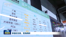
Wow, this is rather interesting on Alibaba T-Head's AI Chip
96GB HBM2e memory, 700 GB/s data-link (noticeably faster than both Ascend-910B and Biren 104P)
Uses PCIe 5.0 and power consumption 400W
Other pic show that 16384 card Alibaba cluster producing 1.945 EFlops
and it seems to come in 16 card per machine. So that's 118 TFLOPS per card.
vs 250 to 320 for Meta-X and Biren card. So, this might be a case where you need more T-Head card, but since they have more memory and fast enough data-linking, that it can be used for training. The per card computation does seem a little underwhelming.
China’s SMIC Begins Trial Operation of 7nm DUV Equipment… Moving Away from ASML Dependence and Pushing Localization-FT According to the Financial Times, China’s largest foundry SMIC is currently trialing a deep ultraviolet (DUV) lithography machine developed by Shanghai-based startup Yuliangsheng (裕量晟). DUV equipment is widely used in semiconductor manufacturing, and until now China had relied heavily on ASML tools. However, with new imports effectively blocked by U.S.-led sanctions, efforts to localize production are accelerating. The new system uses immersion technology, fundamentally supporting the 28nm process. With multiple patterning, it could produce chips down to the 7nm class. Some experts believe attempts at 5nm production might also be possible, though yields and stability would face major limitations. Meanwhile, domestic efforts toward EUV development are also underway. Shenzhen-based SiCarrier is pursuing an EUV lithography project under the codename “Mount Everest.” But this remains at an early stage, and the outlook for real mass production is still highly uncertain. Meanwhile, China’s semiconductor industry has announced plans to triple its production capacity by 2026. However, most of this expansion will inevitably rely on previously acquired ASML DUV equipment, and the newly developed domestic tools are not expected to be deployed in mass production lines until after 2027
FT claims XKL's EUV Project codenamed Mt. Everest
FT claims XKL's EUV Project codenamed Mt. Everest
@tokenanalyst any updates on RSLaser's 90W DUV Laser?
It’s interesting that this report phrases its snippet on EUV as “SiCarrier is pursuing an EUV lithography project” and doesn’t make mention of any other efforts outside the context of SiCarrier.China’s SMIC Begins Trial Operation of 7nm DUV Equipment… Moving Away from ASML Dependence and Pushing Localization-FT According to the Financial Times, China’s largest foundry SMIC is currently trialing a deep ultraviolet (DUV) lithography machine developed by Shanghai-based startup Yuliangsheng (裕量晟). DUV equipment is widely used in semiconductor manufacturing, and until now China had relied heavily on ASML tools. However, with new imports effectively blocked by U.S.-led sanctions, efforts to localize production are accelerating. The new system uses immersion technology, fundamentally supporting the 28nm process. With multiple patterning, it could produce chips down to the 7nm class. Some experts believe attempts at 5nm production might also be possible, though yields and stability would face major limitations. Meanwhile, domestic efforts toward EUV development are also underway. Shenzhen-based SiCarrier is pursuing an EUV lithography project under the codename “Mount Everest.” But this remains at an early stage, and the outlook for real mass production is still highly uncertain. Meanwhile, China’s semiconductor industry has announced plans to triple its production capacity by 2026. However, most of this expansion will inevitably rely on previously acquired ASML DUV equipment, and the newly developed domestic tools are not expected to be deployed in mass production lines until after 2027
FT claims XKL's EUV Project codenamed Mt. Everest
English is not my native language, so I can only provide a rough update using translation software.@tokenanalyst any updates on RSLaser's 90W DUV Laser?
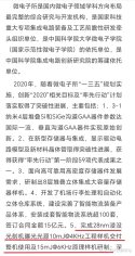
The Institute of Microelectronics of the Chinese Academy of Sciences revealed in its annual report released in 2021 that a 90W laser principle prototype has been delivered in 2020.
The 2021 annual report has been officially removed.
Completed delivery of the 28nm immersion lithography exposure light source engineering prototype at 10mJ@4KHz for full-system operation, and developed the 15mJ@6KHz proof-of-concept prototype.完成28nm浸没光刻机曝光光源10mJ@4KHz工程样机交付整机使用及15mJ@6KHz原理样机研制。

谢谢,this means that the one that said 40-60W is just the earlier iterations of the lithography machine, and surely the lithography machine with the 90W light source have started production now, are there any more updates on RSLaser? Even higher than 90W light source maybe? Thanks in advanceEnglish is not my native language, so I can only provide a rough update using translation software.
The Institute of Microelectronics of the Chinese Academy of Sciences revealed in its annual report released in 2021 that a 90W laser principle prototype has been delivered in 2020.
The 2021 annual report has been officially removed.
Completed delivery of the 28nm immersion lithography exposure light source engineering prototype at 10mJ@4KHz for full-system operation, and developed the 15mJ@6KHz proof-of-concept prototype.
View attachment 160895


