Chinese semiconductor thread II

tokenanalyst

Lieutenant General
Registered Member
Where are you getting 12-15mJ from? The full paper lists 8-12mJ which at 6Hz is 48-72W.
Please, Log in or Register to view URLs content!
15mJ was from CAS post in their website, they delete it, so my second source for the numbers is this paper.
In the paper tested to a ranged of energies with the goal of testing the stability of a new feature of the laser that they are implementing not to push to 15mJ to show off but is pretty clear that they can push this system to higher energies till 15 mJ as CAS stated.
 

ZeEa5KPul

Colonel
Registered Member
15mJ was from CAS post in their website, they delete it, so my second source for the numbers is this paper.
In the paper tested to a ranged of energies with the goal of testing the stability of a new feature of the laser that they are implementing not to push to 15mJ to show off but is pretty clear that they can push this system to higher energies till 15 mJ as CAS stated.
I see. The paper establishes 12mJ per pulse at 6kHz as a lower bound on the laser's capability.
 

tokenanalyst

Lieutenant General
Registered Member

A RISC-V 32-bit microprocessor on two-dimensional semiconductor platform​

Abstract​


With the rapid development of information technology, the demand for high-performance and low-power microprocessors continues to grow. Traditional silicon-based semiconductor technologies have encountered numerous bottlenecks in performance enhancement, such as drain-induced barrier lowering, reduced mobility caused by interface scattering, and limited current on/off ratios. These limitations have spurred researchers to seek out new materials. Two-dimensional (2D) semiconductors have emerged as a promising solution due to their atomic thickness, excellent electrical properties, and mechanical flexibility[1−5]. Despite significant progress in the wafer-scale growth and device fabrication of 2D materials, integrating them into large-scale functional circuits remains a challenge[6−10]. Recently, Zhou and colleagues achieved a significant breakthrough in this area by successfully developing the RV32-WUJI, a RISC-V 32-bit microprocessor based on 5900 molybdenum disulfide (MoS₂) transistors, demonstrating the great potential of 2D semiconductors in complex circuits. This microprocessor achieved a manufacturing yield of 99.77% and a low power consumption of 0.43 mW at an operating frequency of 1 kHz, showcasing the feasibility and efficiency of 2D semiconductor technology in practical applications (Nat. (2025).
1757977395683.png

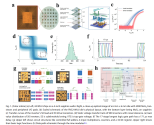
In the manufacturing process, the researchers use a 4-inch MoS₂ wafer to successfully fabricate the RV32-WUJI microprocessor. The microprocessor employs a top-gate field-effect transistor (FET) structure that is compatible with mainstream silicon CMOS technology[12]. The manufacturing process includes front-end-of-line (FEOL) and back-end-of-line (BEOL) processes. By employing a systematic co-optimization strategy and machine learning to analyze the impact of each process step on device performance, the researchers achieve a high yield (99.92% for transistors) and low power consumption (0.43 milliwatts at 1 kHz) in the wafer-scale 2D integrated circuit manufacturing. Fig. 1(a) presents the optical microscopic images of the entire wafer and a single RV32-WUJI chip, highlighting the complexity and scale of the manufacturing. Fig. 1(b) clearly illustrates the four-layer structure of the microprocessor, including the source and drain layer (M0), gate layer, logic connection layer (M1), and module connection layers (M2 and M3), clarifying the functions and interconnections of each layer. This four-layer structure is crucial for achieving the high integration density and functionality required for complex microprocessors. The use of a top-gate structure allows for better control over the electrical properties of the MoS2 transistors, which is essential for high-performance digital circuits. Additionally, the researchers optimize the process flow to ensure compatibility with existing CMOS technologies, making the integration of 2D materials more feasible.

Please, Log in or Register to view URLs content!
 

tokenanalyst

Lieutenant General
Registered Member
Besides the power, NA needs to be 1.35 to go below 28nm
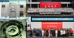
光学投影物镜:由长春国科精密、北京国望光学供应,NA值达0.93,
whats the latest?
To achieve a Hyper-NA,1.35, you need an immersion hood + a combination of mirror and optics.
A think an NA of 0.93 is already at the limit of dry lithography systems, SMEE last High-NA Sub-System was 0.75

1757979194601.png
 

sunnymaxi

Major
Registered Member
To achieve a Hyper-NA,1.35, you need an liquid immersion hood + a combination of mirror and optics.
A think an NA of 0.93 is already at the limit of dry lithography systems, SMEE last High-NA Sub-System was 0.75

View attachment 160809
Untitled.jpg

havok said this in 2023.. SMEE immersion Litho lens is 1.35

Changchun Guoke Precision only produce 0.75 , 0.82 lens.. it is Beijing Guowang Optics that does provide 1.35 NA lens as per havok

0.75/0.82 is fine for dry Lithography.. but for immersion 1.35 is standard.
 
Last edited:

latenlazy

Brigadier
View attachment 160810

havok said this in 2023.. SMEE immersion Litho lens is 1.35

Changchun Guoke Precision only produce 0.75 , 0.82 lens.. it is Beijing Guowang Optics that does provide 1.35 NA lens as per havok

0.75/0.82 is fine for dry Lithography.. but for immersion 1.35 is standard.

The “immersion lens” is a lower than 1.0 NA lens paired with a fluid immersion system (basically a layer of fluid adhering to the lens surface) at the scanning table.
 

def333

New Member
Registered Member
Supposedly, the lithography machine is already fully domestic — SMEE’s first-gen DUVi is on par with ASML’s 1980i, while the second-gen DUVi matches the 2050i.
 
Top