
The Optics Valley team released a nationally produced 12-inch silicon photonics full-process kit, which has entered trial production.
China Optics Valley, on September 11, the National Information Optoelectronics Innovation Center released a domestically produced 12-inch silicon photonics full-process kit (PDK/ADK/TDK). This breakthrough marks the first time that my country has achieved full-process standardization in the field of silicon photonic chips, from design, manufacturing, testing to packaging technology, which can support large-scale mass production of domestically produced silicon photonic chips.
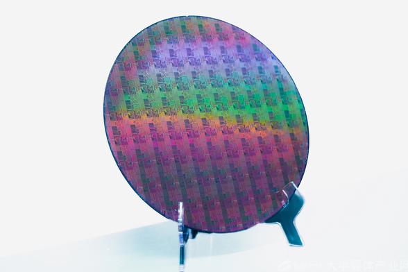
12-inch silicon photonic chip produced using a full-process kit
Compared with traditional microelectronic chips, silicon photonic chips have higher transmission rates and lower power consumption. They are the underlying technology in 5G/6G, AI computing networks, quantum information and other fields. They can also bypass the dependence on EUV lithography machines and achieve "overtaking in another lane" in the chip field.
Chen Daigao, manager of the Silicon Photonics Technology Department at the National Information Optoelectronics Innovation Center, explained that with this full-process suite, all aspects of chip development can use a standardized "language," enabling testing immediately after design and packaging immediately after testing. This avoids repeated verification, shortens the R&D cycle, and reduces manufacturing costs. This technological achievement has already met mass production requirements and is supporting leading companies in pilot production of high-speed silicon photonic chips.
