Chinese semiconductor thread II

tokenanalyst

Lieutenant General
Registered Member

The Optics Valley team released a nationally produced 12-inch silicon photonics full-process kit, which has entered trial production.​


China Optics Valley, on September 11, the National Information Optoelectronics Innovation Center released a domestically produced 12-inch silicon photonics full-process kit (PDK/ADK/TDK). This breakthrough marks the first time that my country has achieved full-process standardization in the field of silicon photonic chips, from design, manufacturing, testing to packaging technology, which can support large-scale mass production of domestically produced silicon photonic chips.
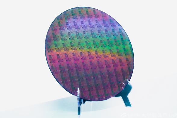
w700d1q75cms.jpg


12-inch silicon photonic chip produced using a full-process kit

Compared with traditional microelectronic chips, silicon photonic chips have higher transmission rates and lower power consumption. They are the underlying technology in 5G/6G, AI computing networks, quantum information and other fields. They can also bypass the dependence on EUV lithography machines and achieve "overtaking in another lane" in the chip field.

Chen Daigao, manager of the Silicon Photonics Technology Department at the National Information Optoelectronics Innovation Center, explained that with this full-process suite, all aspects of chip development can use a standardized "language," enabling testing immediately after design and packaging immediately after testing. This avoids repeated verification, shortens the R&D cycle, and reduces manufacturing costs. This technological achievement has already met mass production requirements and is supporting leading companies in pilot production of high-speed silicon photonic chips.

Please, Log in or Register to view URLs content!
 

tphuang

General
Staff member
Super Moderator
VIP Professional
Registered Member
more on the anti-dumping investigation in American analog chips


I think the increased volume and lower price is probably due to post COVID supply shortage going away as new capacity came online. But it does make sense to do this to help domestic chipmakers which were undercut by TI's aggressive pricing.
 

tokenanalyst

Lieutenant General
Registered Member

TCL Huaxing officially invests in 8.6th generation printed OLED production line, with a total investment of 29.5 billion yuan, only half of the evaporation process.​


TCL Technology Group, through its subsidiary TCL Huaxing, announced a major strategic move in the display industry by signing a cooperation agreement with the Guangzhou municipal government and the Guangzhou Economic and Technological Development Zone. The project involves investing 29.5 billion yuan to build an 8.6th-generation printed OLED production line (the “T8 Project”) in Guangzhou, with a monthly capacity of 22,500 glass substrates (2290mm × 2620mm). The line will produce panels for high-end applications including tablets, laptops, and monitors.

1757782056056.png

Printed OLED Technology: Unlike traditional vacuum evaporation methods, printed OLED uses precise inkjet printing to apply liquid emissive materials directly onto substrates—offering higher material efficiency, lower energy consumption, reduced costs, and scalability across sizes.

TCL Huaxing’s Expertise: With over a decade of R&D in printed OLEDs, TCL Huaxing has already established a successful G5.5 production line in Wuhan (launching mass shipments in November 2024), with capacity ramp-up from 3,000 to 9,000 units/month and continuous improvements in quality and efficiency.

Market Outlook: Global AMOLED panel shipments reached 1.01 billion units in 2024 (27% of total) and are projected to exceed 1.33 billion by 2030 (35% share). Growth is strongest in laptops (+33% CAGR), automotive displays (+27% CAGR), and desktop monitors (+19% CAGR).

Strategic Significance: The T8 project marks a milestone as the first large-scale printed OLED line led by a Chinese company, reinforcing China’s push to dominate next-generation display technology. All technologies used are internally developed, supported by over 9,700 total OLED patents, including more than 1,200 in printed OLEDs—the highest in the industry.

Long-Term Vision: From early R&D in 2013 to commercialization of G5.5 and now T8, TCL Huaxing has built a vertically integrated ecosystem covering materials, equipment, processes, and design—enabling full technological independence and positioning China as a global leader in display innovation.

The project is expected to begin construction soon and will significantly strengthen TCL’s competitive edge in high-end displays while supporting national strategic goals in advanced manufacturing.

Please, Log in or Register to view URLs content!
 

tokenanalyst

Lieutenant General
Registered Member

Henan invests 1.5 billion yuan in high-purity quartz industrialization project​


The project has a total investment of 1.5 billion yuan and will build 20,000 square meters of basic scientific research facilities, including a new mineral material research and development laboratory, a mineral high-efficiency separation test line, and a mineral deep purification test line.
China Powder Network News: Recently, the General Office of the Henan Provincial People's Government issued the "Action Plan for Promoting the Deep Integration of Scientific and Technological Innovation and Industrial Innovation in Henan Province", among which the construction of the Key Laboratory of New Mineral Materials and the high-purity quartz industrialization project were included in the list of key projects.

The project, with a total investment of 1.5 billion yuan, will build 20,000 square meters of basic scientific research facilities, including a new mineral material R&D laboratory, a high-efficiency mineral separation test line, and a deep mineral purification test line. A field research and development base will be established, with proven reserves of at least 10 million tons of high-purity quartz resources and a high-purity quartz mine with an annual production capacity of 900,000 tons. A production line with an annual output of 20,000 tons of ultra-pure quartz sand and 10,000 quartz crucibles will also be built.

Henan Province has inherent advantages in high-purity quartz resources. The granite pegmatite veins exposed in the eastern Qinling Mountains are highly similar to the granite pegmatites in Spruce Pine, North Carolina, USA, a world-renowned high-purity quartz producing area, and have huge resource potential.

The resource scale is considerable: 6,913 granite pegmatite veins have been discovered in the eastern Qinling Mountains, with an average density of about 8.6 veins per square kilometer. Among them, there are nearly 400 medium-to-large pegmatite veins. The two pegmatite-dense areas of Guanpo and Longquanping contain thousands of veins, providing broad space for resource exploration.

Leading quality in China: Purification tests on samples of various pegmatite veins revealed that the total quartz impurity content in the granite pegmatites in this region is less than 100 μg/g overall. The quartz SiO₂ purity of more than 40 veins reaches 4N (99.99%) or higher, with some samples exceeding 4N8 (99.998%), reaching global high-end, high-purity quartz sand standards.

Major breakthrough in ore deposit types: After systematic investigation, the team of Ultrapure Mineral New Materials Industry Technology Research Institute successfully explored and evaluated a 4N8 grade high-purity quartz raw material ore body in the Piaochi Baigantang in the eastern Qinling Mountains, and submitted more than 30 million tons of ore. This is the first time to confirm the existence of Baigantang-type high-purity quartz raw material deposits in the area, laying a resource foundation for large-scale development.

It is worth noting that, relying on the high-purity quartz raw materials of the Baigan type in the Eastern Qinling Mountains, the Institute has produced 4N8 grade high-purity quartz sand in batches through systematic separation and purification experiments. Its various physical and chemical indicators not only meet the domestic "GB/T32649-2016 High-Purity Quartz Sand" standard, but also meet the internationally recognized IOTA-CG (semiconductor-grade quartz raw material) standard. It will effectively solve the problem of dependence on imports of high-end raw materials in my country's semiconductor chip manufacturing, photovoltaic crucible inner layer sand and other fields, and is of strategic significance to ensuring the security of the industrial chain and supply chain.​

Please, Log in or Register to view URLs content!
 

tokenanalyst

Lieutenant General
Registered Member
Advanced EUV Pilot lines for EUV Metal Organic Photoresist.

According to the Wuxi government website, the 2025 Integrated Circuit (Wuxi) Innovation and Development Conference opened on September 4.

Several major projects were announced at this conference. In addition to the computing power platform, there are two other projects worth noting - the Wuxi Advanced Process Semiconductor Nanoscale Photoresist Pilot Line is the first innovative platform in the country to master the core raw materials, formulas and application technologies of MOR-type photoresist. The photoresist it develops and produces will be world-class.

The other is the Jiangsu (Jicui) Photoresist Resin Synthesis Pilot Line, which is the only R&D platform in the country that uses continuous flow technology to prepare photoresist resins. It is the first polymerization equipment and process for the stable synthesis of polymers.

Among them, MOR photoresist is a new technology for photoresist in the EUV era. It refers to metal oxide photoresist, which replaces the CAR chemical amplification photoresist currently used in DUV photoresist. It is one of the key materials for improving photolithography resolution, reducing gate pitch, and reducing defect rate.​
 

jx191

New Member
Registered Member
Any words about revealing EUV machine this month? They are planning to have limited production this month or by the end of year.
Production this year or even this month sounds pretty incredible but a source for that is probably necessary considering the uncertainty surrounding EUV right now
 
Last edited:

jx191

New Member
Registered Member
EUVL Technologies Research (started in 2000) -> EUV Prototypes (2017) -> EUV Pilot Lines(2022-2023?) -> Commercialization and Risk Production (2027-2028?)
I can't seem to find anything on the 2017 prototype systems in this thread or online. All I could find was the talk about prototypes being made much more recently than 2017. Do you know where the 2017 prototype information is?
 

latenlazy

Brigadier
I can't seem to find anything on the 2017 prototype systems in this thread or online. All I could find was the talk about prototypes being made much more recently than 2017. Do you know where the 2017 prototype information is?
The 2017 prototype was just a very simple demonstrator. The more serious commercial project didn’t kick off till maybe 2019-20.
 
Top