Chinese semiconductor thread II

Wrought

Senior Member
Registered Member
So bureaucrats with no technical skills prophesied the advent of the omnipotent machine god and feared the consequences. My god, what a bunch of amateurs.

Key officials believed AI was approaching an inflection point—or several—that could give a nation major military and economic advantages. Some believed a self-improving system or so-called artificial general intelligence could be just over the technical horizon. The risk that China could reach these thresholds first was too great to ignore.

This account of how the Biden administration chose to respond is based on interviews with more than 10 former US officials and policy experts, some of whom spoke on the condition of anonymity to discuss internal government deliberations.

Please, Log in or Register to view URLs content!

I didn't think I could have any more contempt for these people.

For the past few months, I’ve been working closely with Graham Webster, a researcher at Stanford University who sought to understand how and why the Biden team decided the US needed to curb China’s access to advanced semiconductors in the first place. Today, WIRED is publishing Graham’s
Please, Log in or Register to view URLs content!
of what really happened behind the scenes, based on interviews with more than 10 former US officials and policy experts, some of whom spoke on the condition of anonymity.

“I did this piece because the official legal justification for the controls, military and human rights, was obviously never the whole story,” Graham told me. “Clearly AI was in the mix, and I wanted to understand why in some depth.”

Please, Log in or Register to view URLs content!
 

GulfLander

Colonel
Registered Member
China is about to launch SSDs so small you insert them like a SIM card
Chinese storage manufacturer Biwin is calling it the “Mini SSD,” though another manufacturer refers to it as the “1517”; it measures just 15mm x 17mm x 1.4mm thick, smaller than a U.S. penny and just slightly larger than MicroSD. Despite that, it offers maximum sequential read speeds of 3,700 megabytes per second (or 3,400MB/s writes) over a PCIe 4x2 connection, and offers 512GB, 1TB and 2TB capacities.
Please, Log in or Register to view URLs content!
 

tokenanalyst

Brigadier
Registered Member

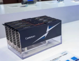
Cambricon: building leading AI software systems​


Cambricon is shaping the future of artificial intelligence by going beyond chip development to build a comprehensive, high-performance AI software ecosystem. As large-scale AI models grow in size and complexity, the demand for powerful yet accessible and reliable infrastructure has never been greater. While Cambricon’s hardware provides the foundational computing power, it is the software that unlocks real-world value—enabling efficient model training and inference, seamless deployment across platforms, and scalable performance.

1755270399543.png

At the heart of this vision is a deeply integrated hardware-software collaboration. The company has developed five generations of intelligent processors and nine specialized AI chips, backed by a robust software platform that spans deep learning frameworks, compilers, operator libraries, distributed communication tools, and end-to-end solutions. This ecosystem allows users to migrate existing models with minimal effort, achieve high performance on Cambricon hardware, and operate efficiently in complex real-world scenarios—such as large language model inference, image and video generation, search, and recommendation systems.

Cambricon is actively building key software components that prioritize usability, performance, and reliability. In framework development, the team maintains strong compatibility with open-source tools like PyTorch and TensorFlow, enabling developers to reuse existing code and debugging practices across different hardware platforms. They continuously optimize the full AI pipeline—from single-card tuning to large-scale distributed training—delivering performance in extreme conditions such as millisecond-level latency or stable operation at 10,000+ GPUs.

The compiler team is developing next-generation toolchains based on MLIR and LLVM, with support for OpenAI’s Triton language and a custom BangC programming language tailored to Cambricon hardware. These tools allow developers to write efficient, high-performance code that fully leverages the chip's architecture.
1755270352609.png

To further simplify development, Cambricon has created an intelligent agent powered by the Deepseek model. This agent can answer technical questions, generate optimized operators in Triton or BangC, and assist users throughout the software development lifecycle—dramatically improving productivity for both new and experienced developers.

Across computing libraries, distributed systems, and inference solutions, the team focuses on maximizing performance through deep optimization at every level: from low-level instruction tuning to high-level parallelism strategies. For example, distributed communication is optimized down to microsecond latency using advanced techniques like remote direct memory access and on-network computation. Inference and training solutions support major models such as Qwen3, DeepSeek, and OpenSora, applying innovations in expert parallelism, data flow optimization, and communication-computation co-design.

The driver team works at the most fundamental layer to optimize kernel performance, memory access patterns, and task scheduling—achieving nanosecond-level efficiency. Their work not only improves current systems but also informs future chip designs by identifying bottlenecks that can be translated into design requirements for next-generation SoCs.

Complementing these technical efforts is a strong focus on reliability. Cambricon’s operations platform enables real-time monitoring, rapid fault diagnosis, and automatic recovery in large-scale clusters—allowing users to detect and resolve issues before launching critical workloads. As cluster sizes grow exponentially, the team prepares for future scalability with robust, forward-looking system design.

Please, Log in or Register to view URLs content!
 

tokenanalyst

Brigadier
Registered Member

Ultrasonic Scanning Microscope + Fully Automatic SAT, Decoding the New Power of Intelligent Manufacturing​


Jinshang Intelligent Technology Jiangsu Co., Ltd. (hereinafter referred to as "Jinshang Intelligent Manufacturing"), established in 2018 and headquartered in Xinwu District, Wuxi, Jiangsu Province, is a high-tech enterprise specializing in the research and development of semiconductor ultrasonic scanning and testing equipment. As a pioneer in domestically produced semiconductor equipment substitution, the company is committed to addressing bottlenecks in the semiconductor industry and has built a product and service system with completely independent intellectual property rights.

The company has a subsidiary in Hefei, Anhui, forming a collaborative business layout between Wuxi and Hefei. With its superior technical expertise and customized service capabilities, Jinshang Intelligent Manufacturing's products have been highly recognized by leading companies in the semiconductor packaging and testing industry, continuously promoting the localization of semiconductor equipment and supporting innovation and development in the industry.


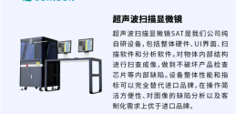
Ultrasonic scanning microscope UTSCAN400
  • Independent research and development: Purely self-developed equipment, covering the overall hardware, UI interface, scanning and analysis software, achieving full independent control from the bottom layer to the application, ensuring technical independence and controllability;​
  • Non-destructive and precise: Scan and image the internal structure of an object, and check for internal defects such as chips without destroying the product, providing a non-destructive and precise solution for electronic component quality inspection;​
  • Import substitution: The overall performance indicators can completely replace imported brands, and are superior to imports in terms of operational simplicity, defect analysis and customization requirements, helping companies reduce costs and increase efficiency, breaking through dependence on imports.​

1755275656569.png

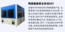
Fully automatic SAT UTSCAN800CLL for ceramic substrates
  • Precision testing: Targeting AMB & DBC ceramic substrates, we conduct specialized testing for voids, delamination, and cracks between copper and ceramic, focusing on industry pain points and ensuring the core quality of substrates.​
  • Efficient collaboration: Seamlessly connect to user tracks, support a variety of material handling, and have functions such as automatic loading and unloading to improve production efficiency and consistency and adapt to production line automation needs;​
  • Full-process support: Equipped with comprehensive functions such as single- and double-sided scanning, drying, and defective product marking and engraving, it provides a complete solution for online full inspection of substrate products and strengthens quality control.​
1755275687855.png

Please, Log in or Register to view URLs content!
 

tokenanalyst

Brigadier
Registered Member

The first domestically produced SiC device bidirectional supercharging pile has been launched in China.​

China's first "360kW/800V bidirectional supercharging pile based on domestically produced silicon carbide components," developed by the technical team of the Production Command Center of the Foshan Power Supply Bureau of Guangdong Power Grid Company, recently passed new product technical appraisal. This achievement achieves three major breakthroughs: fully domestically produced replacement, charging efficiency leaping to 98%, and charging speeds reaching "200 kilometers of range in 5 minutes." This fills a technological gap in domestic silicon carbide high-power charging and discharging, marking a breakthrough in my country's localization and high-performance development of core ultra-fast charging equipment. This milestone holds far-reaching significance for promoting energy transition and supporting the nation's "dual carbon" goals.

The bureau's technical team independently developed the country's most advanced trench silicon carbide devices, successfully producing a charging and discharging device using domestically produced silicon carbide devices with a maximum output power of 360 kilowatts. The core components achieved 100% domestic production. Compared to the 96% peak efficiency of existing charging and discharging equipment, the "domestic bidirectional supercharging station using silicon carbide devices" raises this figure to 98.4%, leading the industry in core performance. With an astonishing "5-minute charge for 200 kilometers of range," it has become a new industry benchmark. For example, a full charge of the Xiaopeng P7 using traditional fast chargers takes at least an hour, but using this technology, it takes only 15 minutes.

In addition, the superior performance of the "bidirectional supercharging pile with domestically produced silicon carbide devices" can also greatly promote the two-way empowerment of V2G. Through the coordinated drive of "vehicle-pile-network-platform", it can effectively promote win-win cooperation among multiple subjects. While reducing social energy consumption costs, it will also further promote the deep integration of urban transportation and energy networks.​


Please, Log in or Register to view URLs content!
 

tokenanalyst

Brigadier
Registered Member
I found many articles written 5 months ago that claimed China will be testing a domestic EUV machine in the second half of 2025.

I don't know how they know this info

Please, Log in or Register to view URLs content!
From my findings is pretty obvious they already have a Machine in trial because a lot of the development in EUV, like EUV mask and EUV reticle handling and stages can only correlate if they already have a machine close to the final product running
 
Top