Chinese semiconductor thread II

tokenanalyst

Brigadier
Registered Member

The Jingkai storage chip packaging and testing project with a total investment of 300 million yuan signed a contract with Xuzhou Economic Development Zone​


On the morning of October 10, Jiangsu Jingkai Semiconductor Technology Co., Ltd. and Xuzhou Economic and Technological Development Zone successfully signed the second phase of the memory chip packaging and testing project, marking another major breakthrough in Jingkai Semiconductor's layout in the semiconductor field. This signing not only demonstrates the company's strength in technological innovation and market expansion, but also injects new vitality into the development of the integrated circuit characteristic industrial cluster in the Economic and Technological Development Zone.

The second phase of Jingkai's memory chip packaging and testing project aims to build an advanced memory chip production line to meet the market's growing demand for high-performance, large-capacity memory chips. The total investment of the signed project is expected to be 300 million yuan, and it is planned to be completed and put into production in the first quarter of 2025. As an important engine for the development of the semiconductor industry in the Huaihai Economic Zone, the Economic Development Zone has become an ideal location for our company's project with its superior geographical location, complete industrial supporting facilities and strong policy support.

Please, Log in or Register to view URLs content!

Please, Log in or Register to view URLs content!
 

tokenanalyst

Brigadier
Registered Member

Shenzhen ASTRI unveils its first 3rd generation semiconductor R&D and testing center​


According to the official WeChat account of the Hong Kong Applied Science and Technology Research Institute (hereinafter referred to as: Hong Kong ASTRI), Hong Kong ASTRI's wholly-owned subsidiary, ASTRI Technology Research (Shenzhen) Co., Ltd. (hereinafter referred to as: Shenzhen ASTRI), moved into the Shenzhen Park of the Hetao Shenzhen-Hong Kong Science and Technology Innovation Cooperation Zone at the beginning of the year and was officially unveiled on October 9.

According to reports, in July last year, the "International Applied Basic Research Institution Project" of the Shenzhen-Hong Kong Science and Technology Innovation Cooperation Zone was officially launched. So far, Shenzhen ASTRI has carried out research and development and testing of multiple projects, mainly focusing on the third-generation semiconductor and new-generation communication technology fields, and established three technology platforms, including the gallium nitride high-end power technology development and testing platform, the silicon carbide intelligent power system development and testing platform, and the smart campus simulation and actual measurement platform, to achieve technology transformation and product commercialization.It is understood that the third-generation semiconductor is a key technology field in Hong Kong in recent years. In May this year, according to Hong Kong media reports, the Finance Committee of the Hong Kong Legislative Council approved a grant of up to HK$2.84 billion (about RMB 2.585 billion) to establish a center focusing on semiconductor research and development - the Hong Kong Microelectronics Research Institute.​

Please, Log in or Register to view URLs content!
 

tokenanalyst

Brigadier
Registered Member

Yujing Co., Ltd.: Silicon carbide substrate cutting, grinding and polishing equipment has achieved batch sales​


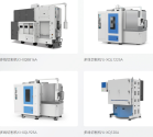
Yujing Co., Ltd. stated that its products used in the semiconductor industry are mainly grinding and polishing machines and multi-wire cutting machine series products. Among them, high-precision CNC cutting, grinding and polishing equipment used in silicon carbide substrate material processing has been sold in batches, making it one of the main suppliers of silicon carbide substrate processing equipment.

1728663583590.png1728663635873.png

Yujing Co., Ltd. said that its ultra-precision cutting and polishing equipment such as multi-wire cutting machines and double-sided polishing machines for 8-inch silicon carbide materials have reached the level of similar imported equipment and have been recognized by customers and the market.

According to official website information, Yujing Co., Ltd. was established in June 1998. It is an intelligent equipment manufacturing company focusing on the photovoltaic, new energy vehicle and consumer electronics industries. It is mainly engaged in the research and development, production and sales of multi-wire cutting machines, grinding and polishing machines and other hard and brittle material processing equipment, diamond wires, thermal field systems and photovoltaic silicon wafer series products.

Yujing Co., Ltd.'s products are mainly used for the precision processing of hard and brittle materials such as solar photovoltaic silicon wafers, sapphire, silicon carbide, mobile phone touch screens and back covers, window glass, LED lighting, magnetic materials, piezoelectric crystals and ceramics. They are widely used in the photovoltaic industry, consumer electronics industry, automotive industry, instrumentation and other industries.

Please, Log in or Register to view URLs content!
 

Wrought

Senior Member
Registered Member
Color me surprised, think tanks are finally catching on. Better late than never, I guess.

U.S. policymakers are increasingly leveraging export controls on advanced semiconductors and related technologies to constrain China’s development of military and dual-use capabilities. But notably, expanding U.S. trade restrictions have heightened political and commercial pressure on Chinese semiconductor companies to wean off U.S. technology wherever possible, with potential negative impacts for U.S. technological leadership. This report, the first in a series of four, explains how export controls have accelerated and scaled Chinese efforts to design out (i.e., adopt alternative sources for U.S. technologies) and design around (i.e., innovate new technologies that bypass U.S. technologies altogether), ultimately facilitating a shift of global semiconductor supply chains away from the United States. This report describes how the design-out and design-around strategies jeopardize U.S. economic and national security due to the diversion of sales and innovation to China and other nations’ technology champions.

Please, Log in or Register to view URLs content!
 

huemens

Junior Member
Registered Member
Color me surprised, think tanks are finally catching on. Better late than never, I guess.


Please, Log in or Register to view URLs content!

"Think tanks" like that write reports according to the requirements of whoever sponsors the report. This reports seems to be sponsored by AMAT who makes a big chunk of their money from China.
This report is made possible through generous support from Applied Materials and ONTO Innovation.

Tomorrow if someone else asks them to make a report in favor of more sanctions, they will write that.
 

tokenanalyst

Brigadier
Registered Member
Color me surprised, think tanks are finally catching on. Better late than never, I guess.


Please, Log in or Register to view URLs content!

"Think tanks" like that write reports according to the requirements of whoever sponsors the report. This reports seems to be sponsored by AMAT who makes a big chunk of their money from China.


Tomorrow if someone else asks them to make a report in favor of more sanctions, they will write that.
The issue with overly zealous export controls damaging US companies and their market share is nothing new, is something that has been study since the nearly the end of the "cold war" so anyone pretending to be shock about export controls backfiring is either ignorant or an ideologue or both.
1728743594689.png1728743645055.png

THE BIG BIG BIG ISSUE about current US export controls is that looks like that intention is to KILL, no even national security anymore and is not the cutting edge anymore, the intention is try to kill Chinese companies and even kill entire Chinese economic sectors, kill Huawei, kill SMIC, kill China memory industry,kill China AI sector, kill China semiconductor industry. THIS IS ECONOMIC WAR and the stooges see US companies as causalities. And you can see it the actions and the language, reducing the des-minimum rule to zero, attacking already established technologies like DUV immersion lithography that China has been buying for two decades, breaking US companies business integrity by banning them from servicing already bought equipment, Alan saying "their tools will ossify" and so on. I don't think even in the Cold War export controls has been this weaponized to harm economic sectors let alone in the post-cold war era.

My hypothesis that the stooges in D.C. WANTS for US semiconductor and technology companies in general market share in China to reach zero or close to zero as possible, that China becomes more independent in chip technology in general, that way the pressure on BIS will diminish or so the stooges think.
 

tokenanalyst

Brigadier
Registered Member

Another Hangzhou chip R&D company completes hundreds of millions of financing.​


Recently, CVSENS successfully completed its A round of financing worth hundreds of millions of yuan. The financing was led by Hanlian Semiconductor Industry Fund, and co-invested with Zhejiang University Education Foundation and Shanghai Anchuang Chuangxin.

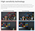
As a leading domestic CMOS image sensor chip development company, it focuses on the design and development of high value-added CMOS image sensor chips.
Currently, more than ten CIS chips have been launched, all of which were successfully taped out at one time, covering multiple application areas such as smart security, low-power IOT, smart cars, and machine vision.
According to official information from CVSENS, it is a high-tech enterprise specializing in the research and development, design and services of CMOS image sensor chip products.
Headquartered in Hangzhou, it has R&D centers and sales offices in Shanghai, Shenzhen, Chengdu and other cities, with more than 100 R&D engineers. The founding team mainly comes from the original overseas top CMOS image sensor core R&D team, of which more than 50 have overseas design experience. They have more than 15 years of R&D and management experience in the high-end CIS field and are responsible for the R&D and design of more than 100 high-end CIS chips. The products cover a wide range of CIS product application fields such as automotive vision, smart security, low-power IoT, machine vision and medical vision.

1728745858518.png

Please, Log in or Register to view URLs content!
 

tokenanalyst

Brigadier
Registered Member

Huancaixing Technology was rated as a national-level specialized and innovative "little giant" enterprise​


Huancaixing Technology (Ningbo) Co., Ltd., a domestic supplier of comprehensive solutions for the industrialization and process technology of AMOLED precision metal masks, was successfully rated as the sixth batch of specialized, sophisticated and innovative "little giant" enterprises by the Ministry of Industry and Information Technology of China. The national-level specialized, sophisticated and innovative "little giant" enterprise is the highest level and most authoritative honorary title in the national small and medium-sized enterprise assessment work. The rated enterprises are located in the core areas of the industrial foundation and the key links of the industrial chain. They have outstanding innovation capabilities, master core technologies, have a high market share in the subdivided market, and have good quality and efficiency. They are the "leading" enterprises in various subdivided industries.

1728747211640.png

Please, Log in or Register to view URLs content!
 

gelgoog

Lieutenant General
Registered Member
I don't think even in the Cold War export controls has been this weaponized to harm economic sectors let alone in the post-cold war era.
The US did the same thing to the Soviet Union. The Soviets ended up buying machine tools from Europe and DRAM chips or MSX computers from Japan.

If you read the reports about the way the Soviets had dealings with the US computer industry it is kind of revealing. For example they had a couple DEC computer machines, but they were kept under lock and key, and were regularly inspected by US inspectors to prevent reverse engineering.

Imports became even more difficult after Carter tightened exports further after the Soviet invasion of Afghanistan.

For example the Soviets were supposed to buy the Lockheed L-1011 TriStar. They had basically agreed on a deal then the US Carter government just came in and put a kibosh on it. The Soviets ended up designing their own Il-86 because of that.
 
Last edited:
Top