Chinese semiconductor thread II

tokenanalyst

Brigadier
Registered Member
mean we don't know this is not true at all.

It was known for a while that yield for delete A lines are lower. It should not surprise anyone that ramping up new production lines have problems. They are doubling capacity in a year. Why would there not be problems along the way?
There is a middle ground, is not saying that they have zero issues, every fab developing new processes and opening new lines is expected to work out things on the way.
The issue is with the mainstream pointing out "unsolvable problems" without any evidence. I think any "unsolvable problem" that SMIC could have it would reflect in their revenue, expansion and in their market share with other domestic fabs like HHGrace who I think have no problems sourcing US tools, what I'm seeing at least from my POV points me to the contrary. Do they have a tough environment? Absolutely yes. But no unsolvable problems.
 

tokenanalyst

Brigadier
Registered Member
Maybe one day we could run DeepSeek 8 bit quants in a PC.​

Huawei releases new AI SSD series, breaking the performance and capacity bottlenecks of traditional AI memory​


On August 27th, Huawei held a new product launch event for its AI data storage SSD in Shanghai. Dr. Zhou Yuefeng, Vice President of Huawei and President of its Data Storage Product Line, unveiled the Huawei OceanDisk EX/SP/LC series of high-end SSDs for the AI era. These products aim to break through the performance and capacity bottlenecks of traditional AI storage, improve AI training efficiency and inference experience, and set a new benchmark in the AI storage field. Huawei also partnered with the Data Storage Committee of the China Electronics Standardization Association, the Shanghai Institute of Artificial Intelligence, and several partners to jointly launch the "AI SSD Innovation Alliance" to continuously promote industry ecosystem collaboration and technological innovation.

With the rapid adoption of AI applications, data corpora are evolving from "plain text" to "multimodal," exponentially increasing in size. Inference text is shifting from "short sequences" to "multimodal fusion long sequences," further deteriorating the AI inference experience. Zhou Yuefeng stated, "The increasingly severe 'memory wall' and 'capacity wall' have become key bottlenecks to AI training and inference efficiency and user experience. This poses significant challenges to the performance and cost of IT infrastructure, impacting the positive AI business cycle."

Huawei's new AI SSDs are high-performance, large-capacity solid-state drives optimized for AI workloads. They come in three types: extreme performance, high-performance, and large-capacity.

Huawei OceanDisk EX 560 (Extreme Performance Drive): Provides extreme performance, with random write performance of up to 1,500K IOPS, random write latency of less than 7µs, and endurance of up to 60 DWPD (Full Drive Writes Per Day).
Ideal for AI all-in-one training scenarios, the high-performance AI SSD increases the number of fine-tunable model parameters on a single machine by six times, enabling easy fine-tuning of large models with hundreds of billions of parameters.

Huawei OceanDisk SP 560 (High-Performance Drive): Offers high cost-performance, with random write performance up to 600K IOPS, random write latency below 7µs, and endurance of 1 DWPD. Suitable for inference scenarios in all-in-one machines and clusters, it increases the inference sequence length by 2.5 times, further optimizing the inference experience and costs, achieving a 1-2x increase in TPS and a 75% reduction in first-token latency.

Huawei OceanDisk LC 560 (Large Capacity Drive): Offers ultra-large capacity, with a maximum single-drive physical capacity of 245TB and a read bandwidth of up to 14.7GB/s. It is suitable for cluster training scenarios, helping to increase data collection and preprocessing efficiency by 6.6 times, enabling efficient storage of massive multimodal corpora.
Huawei also launched DiskBooster driver software, which supports intelligent collaboration between AI SSDs and HBM and DDR memory, achieving a 20-fold expansion of virtual pooled memory through memory expansion technology. The software also features intelligent multi-stream technology that works with upper-layer applications to effectively reduce write amplification effects and further extend the lifespan of AI SSDs.

Please, Log in or Register to view URLs content!
 

sunnymaxi

Major
Registered Member
I mean we don't know this is not true at all.

It was known for a while that yield for delete A lines are lower. It should not surprise anyone that ramping up new production lines have problems. They are doubling capacity in a year. Why would there not be problems along the way?
the article says, SMIC has lack of testing equipment which delaying the expansion for at least 6 months.. i replied, no its not true.. Si Carrier, Jingce , SMEE and Angstorm-E testing/Metrology tools entered in full production.

i m not denying production problem and reliability of domestic tools.
 

tokenanalyst

Brigadier
Registered Member

Room-temperature bonding breakthrough! SiC-based lithium niobate thin films help SAW enter the high-frequency era​


As 5G evolves into millimeter-wave bands and radar systems demand higher performance, traditional surface acoustic wave (SAW) filters are limited to frequencies below 3 GHz due to substrate constraints. Bulk acoustic wave (BAW) technology offers higher frequency operation but faces high costs and poor thermal stability.

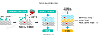
Qinghe Jingyuan Semiconductor Technology (Group) Co., Ltd. has developed a silicon carbide (SiC)-based lithium niobate (LiNbO₃) thin film substrate using proprietary room-temperature bonding technology, enabling SAW devices to operate efficiently in high-frequency applications—marking a major leap forward for RF filtering.
1756757834104.png

Key performance highlights:

-Resonator Qmax reaches 710 at 5 GHz
-Electromechanical coupling coefficient (K²) exceeds 20%
-Strong RF performance across critical 5G bands including N77 and N78

The technology overcomes the challenges of bonding SiC and LiNbO₃—materials with significant thermal expansion differences—through surface activated bonding (SAB) under ultra-high vacuum at room temperature.

Core innovations:


-Atomic-level interface control: surface roughness < 0.5 nm, enabling covalent bond formation
-Eliminates thermal mismatch stress by avoiding high-temperature processing
-High-precision alignment with ±1 μm mark accuracy and pressure uniformity within ±3%
-Bond strength exceeds 10 MPa across the entire interface

The solution has achieved large-scale production of 6-inch SiC/LiNbO₃ wafers, with mass production yield exceeding 95%. It is already validated for use in existing 5G systems and poised for wider deployment.

Qinghe Jingyuan is a high-tech leader in semiconductor bonding and integration. The company specializes in advanced packaging, heterogeneous material integration, MEMS sensors, and wafer-level processes. Through its dual-engine model of equipment development and process services, it offers fully integrated solutions with proprietary technology across four product lines.

This breakthrough positions SiC/LiNbO₃ as a scalable, high-performance alternative to BAW—accelerating innovation in 5G-Advanced, 6G, and beyond.

-Reduces filter manufacturing costs by over 30% compared to BAW
-Expands operating temperature range by up to 50%
-Enables next-generation applications in millimeter-wave communications, satellite internet, and intelligent driving radar

Please, Log in or Register to view URLs content!
 

tokenanalyst

Brigadier
Registered Member

Hunan Sanan achieves new breakthrough in silicon carbide device field​

According to recent media reports, Hunan San'an Semiconductor (hereinafter referred to as "Hunan San'an") officially launched its first generation of high-performance Trench MOSFET technology platform in August this year, achieving a major technological breakthrough in the field of silicon carbide power devices.

Hunan San'an's Trench MOSFET technology platform boasts an on-resistance as low as 1.75 mΩ·cm² and a breakdown voltage exceeding 1400V, achieving industry-leading core static performance. Furthermore, Hunan San'an plans to further reduce the on-resistance of its next-generation products by over 20%.

It is reported that the above-mentioned technology platform has passed the electrical performance screening and reliability testing, and core data such as gate oxide quality have excellent performance, which can meet high-requirement application scenarios such as new energy vehicles, photovoltaic inverters, and industrial power supplies.

In the future, Hunan San'an will continue to deepen its research and development of silicon carbide technology and accelerate the large-scale application of third-generation semiconductors in energy transformation and high-end manufacturing.

Please, Log in or Register to view URLs content!
 

jx191

Just Hatched
Registered Member
I spent some time today reading the points made by @nativechicken about the current state of EUV in China and the difference between the information and speculation on here is so different to what the western media reports. His points were really interesting and I agree that EUV instability would be tolerated as opposed to the DUVi processes when it comes to that stage.

For example, @nativechicken claims that EUV prototypes are entering an acceptance phase and that some forms of production will be ready very soon, whereas there is absolutely nothing from western media about anything like that, apart from a few rumours on X that made their way into some articles.

Is opsec really that tight in China? Surely talking about how Chinese EUV machines are actually nearing production here would attract more attention from the people who still think China is 20 years behind in lithography.
 

tokenanalyst

Brigadier
Registered Member
I spent some time today reading the points made by @nativechicken about the current state of EUV in China and the difference between the information and speculation on here is so different to what the western media reports. His points were really interesting and I agree that EUV instability would be tolerated as opposed to the DUVi processes when it comes to that stage.

For example, @nativechicken claims that EUV prototypes are entering an acceptance phase and that some forms of production will be ready very soon, whereas there is absolutely nothing from western media about anything like that, apart from a few rumours on X that made their way into some articles.

Is opsec really that tight in China? Surely talking about how Chinese EUV machines are actually nearing production here would attract more attention from the people who still think China is 20 years behind in lithography.
My position is that EUV is probably entering the trial stage given the quantity of information of EUV masks, photoresist, defect detection and reticle information that is coming out. They are going high, according to a "semi-authoritative" source that I posted here.

Immersion lithography scanners are already in production and they still iterating towards 7nm process nodes, I found information in a government website about ultrapure liquid filtering technology for 14nm for immersion lithography technology to be deployed this year. That I think means whatever these machines are they are being used for a 14nm process node.
 

latenlazy

Brigadier
Is opsec really that tight in China? Surely talking about how Chinese EUV machines are actually nearing production here would attract more attention from the people who still think China is 20 years behind in lithography.
Yes. Even as the work has become harder to hide and the circles of people involved continue expanding the frequent story whenever someone adjacent to the industry is asked is “can’t talk about it”. No one saw SiCarrier’s giant April equipment drop for example.
 
Top