Chinese semiconductor thread II

measuredingabens

Junior Member
Registered Member

Van der Waals quaternary oxides for tunable low-loss anisotropic polaritonic​

Abstract
The discovery of ultraconfined polaritons with extreme anisotropy in a number of van der Waals (vdW) materials has unlocked new prospects for nanophotonic and optoelectronic applications. However, the range of suitable materials for specific applications remains limited. Here we introduce tellurite molybdenum quaternary oxides—which possess non-centrosymmetric crystal structures and extraordinary nonlinear optical properties—as a highly promising vdW family of materials for tunable low-loss anisotropic polaritonics. By employing chemical flux growth and exfoliation techniques, we successfully fabricate high-quality vdW layers of various compounds, including MgTeMoO6, ZnTeMoO6, MnTeMoO6 and CdTeMoO6. We show that these quaternary vdW oxides possess two distinct types of in-plane anisotropic polaritons: slab-confined and edge-confined modes. By leveraging metal cation substitutions, we establish a systematic strategy to finely tune the in-plane polariton propagation, resulting in the selective emergence of circular, elliptical or hyperbolic polariton dispersion, accompanied by ultraslow group velocities (0.0003c) and long lifetimes (5 ps). Moreover, Reststrahlen bands of these quaternary oxides naturally overlap that of α-MoO3, providing opportunities for integration. As an example, we demonstrate that combining α-MoO3 (an in-plane hyperbolic material) with CdTeMoO6 (an in-plane isotropic material) in a heterostructure facilitates collimated, diffractionless polariton propagation. Quaternary oxides expand the family of anisotropic vdW polaritons considerably, and with it, the range of nanophotonics applications that can be envisioned.

Please, Log in or Register to view URLs content!
 

measuredingabens

Junior Member
Registered Member
Two-dimensional perovskite oxide as a photoactive high-κ gate dielectric

Abstract​

High dielectric constant (high-κ) gate dielectrics compatible with two-dimensional (2D) semiconductors are essential for scaled optoelectronic devices. However, conventional three-dimensional dielectrics are difficult to integrate with 2D materials with dangling-bond-free surfaces. Here we show that the 2D perovskite oxide Sr2Nb3O10, prepared by a top-down approach, can be integrated with various 2D channel materials. The high dielectric constant (24.6) and moderate bandgap of Sr2Nb3O10 allow it to be used as a photoactive high-κ dielectric for phototransistors with various 2D channel materials, including graphene, molybdenum disulfide, tungsten disulfide and tungsten diselenide. Molybdenum disulfide transistors exhibit an on/off ratio of 106 with a supply voltage of 2 V and a subthreshold swing of 88 mV dec−1. Tungsten disulfide phototransistors exhibit a photocurrent-to-dark-current ratio of ~106 and ultraviolet (UV) responsivity of 5.5 × 103 A W−1 under visible or UV light illumination, due to the combined effect of gate control and charge transfer from the photoactive gate dielectric. We also show that the phototransistors with the photoactive dielectric can offer UV–visible dual-band photodetection, where UV and visible light illumination are distinguished at separate terminals.

Please, Log in or Register to view URLs content!
 

generalmeng

New Member
Registered Member
There seems to be an argument online which claims China spend less on R&D for semiconductors than usa, Japan, Korea and Taiwan, even though those are smaller states.

I wasn't able to find specific source to back this up. All I found was % of sale as part of R&D. This % is very miss-leading as China have almost 50% of the global export, so imo small% of a very large number is still a very large number.

I was not able to find any nominal number for comparison. Did some one else also come to the same question, and did you find an answer? Nominal spending comparison between all the countries.
 

tokenanalyst

Brigadier
Registered Member
Ultra High energy Ion Implanters for sensors, compound semis and logic.​

The localization of high-energy ion implanters achieves new breakthroughs in Qingdao​


At the beginning of the new year, Qingdao Sifang Sirui Intelligent Technology Co., Ltd. (hereinafter referred to as "Sirui Intelligence") located in the Qingdao intelligent Manufacturing Valley has increased the horsepower of its production line to carry out large-scale production and assembly of high-energy ion implanters.
Last year, Sirui Intelligent successfully developed the country's first high-energy ion implanter with an energy of 8 MeV (megaelectron volts) and successfully delivered it to a leading domestic company. This means that domestic integrated circuit core manufacturing equipment has achieved a major breakthrough, not only filling the gap The domestic gap has also broken the technological blockade of Western countries, opening up a new journey of independent and controllable domestic high-energy ion implanters, adding equipment support to the high-quality development of the integrated circuit industry.

Covering an area of 48 square meters and weighing 38 tons, the SIRUI intelligent high-energy ion implanter looks like an ordinary large-scale production equipment in an industrial workshop. This seemingly ordinary machine is actually the core manufacturing equipment of integrated circuits. For a time, the localization rate was zero, which restricted the independent controllability of my country's integrated circuit industry chain.

A high-energy ion implanter is required to increase the ion energy to nearly 10 million electron volts. It requires the coordinated work of more than a dozen acceleration systems, involving dozens of joint adjustment parameters, and ultimately achieves deep implantation and doping of heavy ions at the micron level before it can be applied to power applications. Preparation of main components of integrated circuits such as devices, IGBTs, CMOS image sensors, 5G RF, logic chips, etc.

Led by technological innovation to promote new industrialization, Sirui Intelligent's products have been promoted and applied by leading chip manufacturing companies. It is expected that by the end of the "14th Five-Year Plan", it will have a large-scale production capacity of 50 units per year, with an output value of over 1 billion yuan. . This achievement has effectively promoted the rapid development of my country's integrated circuit manufacturing equipment and effectively guaranteed the independence and controllability of the semiconductor industry chain.

1709395425197.png

Please, Log in or Register to view URLs content!
 

tokenanalyst

Brigadier
Registered Member
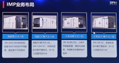
The field of ion implantation is getting basically covered in China. From low current, medium current and high current. Low energy, medium energy and high energy. High dose.

SRII
Covering compound, imaging sensors, RF and logic.
1709396987657.png


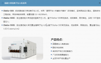
Wanye:
Covering PV, compound, logic and so on.
low energy.

1709396087214.png
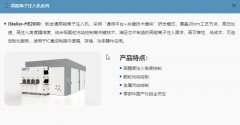
High energy:
1709396204580.png

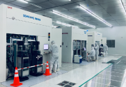
CETC/SEMICORE:
They have a good coverage from Ion Implanters for SiC and compound semis to Ion Implanters for IC logic manufacturing.

1709396513589.png

Please, Log in or Register to view URLs content!

A lot of competition to move the industry to more advanced nodes, staying in the same "mature nodes" is becoming NOT an option for Chinese equipment manufacturers.
It will be interesting if in the future SMEE would have this same pressure from peer competitors.
 

bebops

Junior Member
Registered Member
There seems to be an argument online which claims China spend less on R&D for semiconductors than usa, Japan, Korea and Taiwan, even though those are smaller states.
not surprised. it is called bigger bang for your buck. you can get alot for a buck if you spend it elsewhere.
 

tokenanalyst

Brigadier
Registered Member

Guoji Southern and 55th Institute: Accelerate technological research on silicon carbide MOSFET, with shipments exceeding 15 million units​


MBXY-CR-52a2b2bb25b6bd053303550947b6a259.png


"With the increase in supply and demand of new energy vehicles, we are also accelerating the research and mass production of key core technologies for high-current silicon carbide MOSFETs." During the Spring Festival, the team started early and stuck to their posts, focusing on new energy vehicles, photovoltaics, and high-voltage transmission and transformation. The demand in key areas such as electricity and smart grids ushered in spring amid the hot production.

Silicon carbide MOSFET can increase the charging speed of new energy vehicles by 5-10 times, increase the cruising range by more than 8%, and reduce energy consumption by 50%. Its excellent performance makes it a key component required for new energy vehicles. Up to now, the shipment volume of the 650V-1200V silicon carbide MOSFET for new energy vehicles developed by the team has exceeded 15 million units, and a total of more than 2 million units have been put on the vehicle.

the silicon carbide teams of Guoji Southern and 55 Institute have penetrated the mass production platform of the entire industry chain such as silicon carbide substrates, epitaxy, and chips, and have successively broken through high-temperature and high-energy ion implantation, high mobility Gate oxidation and other key processes.
After gathering wisdom and hard work, the team established the first 6-inch silicon carbide power product production line in China, became the first in China to break through the 6-inch silicon carbide MOSFET mass production technology, and formed a complete set of silicon carbide power product technology systems with independent intellectual property rights.

"Significantly improving the yield rate of typical products, we have transformed the silicon carbide products we developed from laboratory samples into batch commercial products, effectively resolving the core shortage crisis for car companies." "To achieve rapid mass production applications, we face great challenges." In order to meet user needs, the team worked non-stop with new energy vehicle companies to dock application requirements, quickly completed product development and verification, and quickly developed silicon carbide MOSFET products with better performance.

"The chip area has been reduced by 30%, and the conduction loss has been reduced by 15%. The power conversion efficiency of the new generation silicon carbide MOSFET products has been significantly improved, and it has entered large-scale application by leading new energy vehicle companies." Experts said that since the product has been verified by user vehicle projects, Silicon carbide MOSFETs are delivered in stable batches every month and won the "Most Influential Automotive Chip Award".
Please, Log in or Register to view URLs content!
 

tokenanalyst

Brigadier
Registered Member

De'Longhi Laser: Orders will grow significantly in 2023, accounting for approximately 50% of the SiC laser slicing equipment market​


1709408206747.png

Delonghi Laser announced its 2023 annual performance report, stating that during the reporting period, it achieved total operating income of 580 million yuan , a year-on-year increase of 2.35%; total assets were approximately 1.7 billion yuan, a year-on-year increase of 8.3%.
According to the report, the main factor affecting operating performance is that Delong Laser has continued to increase investment in research and development in the past two years, and has successfully developed a number of new products and technologies in the direction of semiconductors and new energy, benefiting from silicon carbide crystal laser slicing equipment. , MicroLED mass transfer equipment, perovskite thin film solar cell laser processing equipment, and advanced packaging-related laser processing equipment and other new products have been launched on the market one after another. The company's order growth rate will be obvious in 2023.
De'Longhi Laser focuses on high-end laser equipment and fine micro-machining, and is the only domestic supplier of SiC slicing equipment. Diamond wire cutting has high efficiency and less pollution, and is gradually replacing mortar cutting. Laser slicing has less loss and high efficiency, and is expected to replace diamond wire and become a new generation of mainstream cutting technology. In the existing SiC laser slicing equipment market, due to the high entry barriers in the semiconductor industry, there will be no other obvious competitors in the short term.
According to predictions from Soochow Securities, it is expected that by 2025, the global/domestic new market space for 6-inch SiC slicing equipment will be approximately 3.0/1.3 billion yuan. In terms of diamond wire cutting, Gaoche Co., Ltd. has launched SiC diamond wire slicing machines that are compatible with 4-8 inches. And continue to promote domestic substitution. In terms of laser cutting, Han's Laser and De'Longhi Laser each account for about 50% of the market share .
De'Longhi Laser began to enter the SiC field in 2018. The stress-induced cutting method developed is good at cutting ultra-hard and ultra-brittle materials, and has successfully used this method to achieve high-quality and rapid cutting of SiC wafers.
The Inducer-5560 SiC wafer dicing equipment developed by Delonghi Laser has multiple process advantages. For mainstream 6-inch SiC wafers, the maximum cutting speed is 500 mm/s. The process is mature and can be used to cut SiC wafers for microwave devices and power devices in aerospace, power electronics and other industries.

 
Top