You are using an out of date browser. It may not display this or other websites correctly.
You should upgrade or use an alternative browser.
You should upgrade or use an alternative browser.
Chinese semiconductor thread II
- Thread starter vincent
- Start date
Northern Huachuang : Silicon carbide epitaxy equipment has been sold in batches
Northern Huachuang stated on the investor interactive platform that the company's silicon carbide epitaxial equipment has achieved batch sales, and its market share has always been at the forefront of the country.
NAURA advances in PVD (Physical Vapor Deposition) equipment.
As a pioneer in China's PVD process equipment technology, Northern Huazhuang started the research and development of PVD equipment as early as 2008. After sixteen years of technological accumulation and innovative breakthroughs, it has released a number of mass-produced PVD equipment, with cumulative shipments With over a thousand cavities, it has become the largest solution provider of PVD equipment in China
Since its establishment, Northern Huachuang's PVD Division has made breakthroughs in many key technologies such as magnetron sputtering source design, plasma generation and control, chamber design and simulation, particle control, and software control, and has established core technological advantages. It has achieved the industrialization of equipment and process coverage of metallization processes for logic chips and memory chips. As of the end of 2023, process equipment such as Cu (copper) interconnection, Al Pad (aluminum pad), Metal Hardmask (metal hardmask), Metal Gate (metal gate), and Silicide (silicide) in the integrated circuit field are stable at the client end It has been put into mass production and has become the baseline equipment for many customers, and has become the industry's first choice. Among them, Metal Gate (metal gate) PVD products have successfully achieved mass production breakthroughs in the 28nm metal gate core process; Cu (copper) interconnection PVD products support Inter Metal (internal interconnection lines) and Top Metal (top interconnection lines) Mass production of processes; Al (aluminum) PVD products are used in large quantities in different fields such as logic, DRAM (dynamic random access memory), 3D NAND (flash memory), covering all processes such as Pad (aluminum pad), RDL (redistribution layer), etc. application.
By the end of 2023, the Northern Huachuang PVD team has developed more than 30 systematic equipment solutions for metallized film deposition processes in the pan-semiconductor field. Among them, thermal Al PVD products have excellent Al filling capabilities, and back gold PVD products have good warpage control capabilities. Both PVD products have been fully used in the mass production of power semiconductor front and back electrode processes; Ti, Cu, TSV PVD products such as TiN, Al, AlN, ITO and other PVD products are used in mass production of advanced packaging UBM, RDL, and TSV processes by virtue of their core advantageous technologies such as low temperature, low damage, and high coverage. Features such as roughness, low stress, and high crystal quality strongly support the R&D and mass production of customers in the fields of silicon-based micro-displays, MEMS, and semiconductor lighting.
Loongson's LG200 GPU core should complete development this year. Now in testing.龙芯第二代GPU核LG200将在2K3000中应用,支持图形加速、科学计算加速、AI加速。2K3000计划在今年上半年交付流片。在此基础上,后续将基于2K3000的GPGPU技术及3C6000的龙链技术,研制专用GPGPU芯片
2K3000 will be taped out in first half of this year.
3C6000 will also come out using LoongLink.
2K3000 is octacore CPU designed for desktops/laptops
More SiC news
SMEC says it anticipated 1B RMB in SiC revenue this year. Huge growth area for them
CETC 55th institute is now testing and getting their SiC MOSFET ready for NEVs. It claims that its SiC MOSFET has already been used on over 2million EVs.
SiC MOSFET improves charging by 5 to 10 times, 8% longer range & 50% lower energy consumption (although this really depends on packaging, eDrive itself, a bunch of factors)
A 2mmx2mm SiC MOSFET is used for EV's OBCs. It's dimension is just 1/10 of Si product of same usage, resistance is 1% of Si & total energy loss can be reduced by 70%
Claims to be the first domestic firm to mass produce 6-inch SiC MOSFET & establish 6-inch SiC production line
New generation SiC MOSFET further reduced chip size by 30% & conduction loss by 15% -> improving power conversion efficiency
They have entire lineup of SiC product from 650V to 6500V for charging, HV power supply, on board charger and radar power supply
Looking to sell more for not only EVs, but also wind/solar poer, ESS & grid.
The damage was done. The US and Micron disrupted Fujian Jinhua's R&D and production. 5 years is an eternity in semis. And even if Fujian Jinhua gets removed from the blacklist they still won't be getting the latest 18nm and better tools for DRAM since sales of those to China is now banned.So some guy here ended being wrong. So don't expect no even an apology from the stooges in D.C. Jinhua should not expect that export controls are going to be relaxed and even then they best bet is keep working with local suppliers to secure their supply chain.
I think Loongson should just make RISC-V compatible processors. But whatever.not great year for Loongson despite the new products
revenue don 31% YoY. margins thinks in the negative. R&D up 36.3%
Let's hope this turns around in 2024
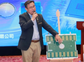
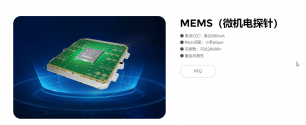
Jingsheng Microna launches N800 ultra-large-scale AI computing power chip test probe card
It is reported that Suzhou Jingsheng Micro-Nano, a subsidiary of Shanghai Taosheng Technology, has launched the N800 ultra-large-scale AI computing power chip test probe card (UltraScale MEMs Probe Card), which uses embedded alloy nano-stack technology and is specially used to achieve ultra-high density and extremely small spacing. The chip testing meets the requirements of high computing power AI chips with high current, high pin count, large card size and high-speed communication interface.
In 2023 Suzhou Jingsheng Micro-Nano Semiconductor, a subsidiary of Shanghai Taosheng Technology, launched an emergency N90 MEMS Cobra probe. This probe covers most of the specifications, performance and features of the classic Cobra probe, and on this basis shortens the process flow, improves manufacturing accuracy, improves high parallelism of testing, greatly reduces testing costs, and effectively solves the problem of high-end chip current Large, power consumption, high frequency, large number of pins and other requirements, and provide high and low temperature test environment. This probe card product is also suitable for the large-scale manufacturing of emerging industry chips such as automotive chips and logistics chips, and provides advanced testing products and a good testing environment for mainstream chip products in China's AI chip industry such as GPU, FGPA, and ASIC.


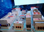
Interesting photo from 2020 which encapsulate the main semiconductor fabrication tools at the time, there is some missing tools in the photo but I know they had at the time like chemical mechanical polishing, but my suspicion is that it was possible to produce chips for quite some time domestically.
Now this has been enhanced significantly with the introduction of more equipment, such more metrology tools like ADI and AEI tools, more CDSEM tools, Optical CD tools, more deposition tools like NAURA Cu tools and AMEC WCVD, Annealing tools, more completion in the ion implantation scene, advance CMP tools, Epitaxial tools, better selective etching tools and so on, along with the new generation Dry and Immersion lithography scanners.

Now this has been enhanced significantly with the introduction of more equipment, such more metrology tools like ADI and AEI tools, more CDSEM tools, Optical CD tools, more deposition tools like NAURA Cu tools and AMEC WCVD, Annealing tools, more completion in the ion implantation scene, advance CMP tools, Epitaxial tools, better selective etching tools and so on, along with the new generation Dry and Immersion lithography scanners.

Quite credible rumors that HW took over Jinhua and started mass production a while agoThe damage was done. The US and Micron disrupted Fujian Jinhua's R&D and production. 5 years is an eternity in semis. And even if Fujian Jinhua gets removed from the blacklist they still won't be getting the latest 18nm and better tools for DRAM since sales of those to China is now banned.
I think Loongson should just make RISC-V compatible processors. But whatever.
