It depend on break through in new generation semiconductor material, who choose the right path, but at least 20 years if China is the right one.Based on the development of last 5 years or so, how long do you guys think China becomes dominant in Semiconductor just like they are in EV right now?
3 to 4 years perhaps?
You are using an out of date browser. It may not display this or other websites correctly.
You should upgrade or use an alternative browser.
You should upgrade or use an alternative browser.
Chinese semiconductor thread II
- Thread starter vincent
- Start date
My take if Trump continued to restrict the Chinese regarding trade and semiconductor then within 5 years it will accelerate and may see a complete domination by 2035.
Sound too optimistic? Well the CPC had just laid out their MADE IN CHINA 2035, just like all their previous 5 year plan, majority of those goals had been realized, now this time with strong scientific and technical foundation being established from the previous 14th plan, I'm extremely confident that the Chinese may achieved complete dominance in certain sector and parity in some like EUVL.
Sound too optimistic? Well the CPC had just laid out their MADE IN CHINA 2035, just like all their previous 5 year plan, majority of those goals had been realized, now this time with strong scientific and technical foundation being established from the previous 14th plan, I'm extremely confident that the Chinese may achieved complete dominance in certain sector and parity in some like EUVL.
The most important assets in semiconductors are not just technology, but also a sufficient talent pool. For China to build a semiconductor system comparable to Taiwan’s would take 15 years, and would also require establishing a supply chain for manufacturing equipment. Overall, this is a task that would take a generation.My take if Trump continued to restrict the Chinese regarding trade and semiconductor then within 5 years it will accelerate and may see a complete domination by 2035.
Sound too optimistic? Well the CPC had just laid out their MADE IN CHINA 2035, just like all their previous 5 year plan, majority of those goals had been realized, now this time with strong scientific and technical foundation being established from the previous 14th plan, I'm extremely confident that the Chinese may achieved complete dominance in certain sector and parity in some like EUVL.
Yes correct that's the main theme of Made in China 2035 as they had address it since 2021 part of the 14th five year plan, its now 2025 and we may see the first batch of graduate entering the work force.The most important assets in semiconductors are not just technology, but also a sufficient talent pool. For China to build a semiconductor system comparable to Taiwan’s would take 15 years, and would also require establishing a supply chain for manufacturing equipment. Overall, this is a task that would take a generation.
Now what about the 15th 5 year plan? Your guess is as good as mine, they will double down and Achieved its goal by 2035.
The 15th Five-Year Plan, which will cover the period from 2026 to 2030, is expected to focus on improving economic resilience, boosting China's technology and innovation capabilities, and will be approved during a CPC Central Committee plenum expected to take place in the fall.21 hours ago
Apr 22, 2021 — Tsinghua University, one of China's top universities, established the School of Integrated Circuits on Thursday, the nation's first, to target research and the ...
Once they catch up in EUV it would be over for rest of the world. China has the supply chain to scale up rapidly and outcompete foreign competitors. I would say with in 10 yearsBased on the development of last 5 years or so, how long do you guys think China becomes dominant in Semiconductor just like they are in EV right now?
3 to 4 years perhaps?
Hefei Xinyihua completed over 300 million yuan in B+ round financing and is a domestic pan-semiconductor high-end equipment manufacturer.
Hefei Xinyihua Intelligent Machinery Co., Ltd. (hereinafter referred to as "Xinyihuazhi"), a pan-semiconductor high-end equipment manufacturer, completed a B+ round of investment of over 300 million yuan. The investment was made by China Development Bank Manufacturing Transformation and Upgrading Fund, Chaoxi Capital, Anhui High-tech Investment, Guozhong Capital, Ultra-High Definition Video Industry Investment Fund, Jinan Yuntong, etc.
According to public information, Xinyi Huazhi was established in 2013 and is an advanced pan-semiconductor high-end equipment provider in China. It mainly engages in the research and development, production, sales and technical services of pan-semiconductor transfer equipment, process and testing equipment, industrial software and big data products. Its business covers strategic emerging industries such as display panels, integrated circuits, and next-generation perovskite photovoltaic cells. The company has established close cooperative relations with more than 100 upstream and downstream customers in the pan-semiconductor industry chain around the world, and has deeply bound with leading companies in various fields to jointly promote the continuous iteration and upgrading of industry processes and equipment technologies.
Xinyi Huazhi is committed to solving the "bottleneck" problem of pan-semiconductor equipment. Since its establishment, the company has successfully launched a number of high-end equipment that fill domestic gaps, breaking the foreign technology monopoly, and its technology level is comparable to that of international leading companies. Many of the company's core products have been selected into the national first major technical equipment promotion and application guidance catalog and passed the Anhui Province's first major technical equipment certification, demonstrating its leading position in the field of high-end equipment.
Xinyi Huazhi relies on the three strategic technology platforms of clean transfer, high-speed and high-precision, and vacuum coating to independently develop a series of high-end equipment such as semiconductor AMHS, high-speed and high-precision patch equipment, OLED and perovskite evaporation equipment. After the original various types of panel equipment were gradually localized, the company successfully expanded the photovoltaic perovskite and integrated circuit equipment business, built a diversified growth engine, and has developed into a platform-type equipment leader across the display panel, integrated circuit and photovoltaic fields.
Jinghu Technology has completed a new round of financing of tens of millions of yuan and is a domestic high-end quartz crystal material manufacturer
Recently, Shandong Jinghu Technology Co., Ltd. ("Jinghu Technology"), a domestic high-end quartz crystal material R&D and manufacturing company, completed a new round of financing of tens of millions of yuan, jointly invested by Yingshang Advantage Fund and Fuxin Optoelectronics Fund. This round of funds will be used for upgrading large-size quartz crystal mass production equipment, R&D investment and capacity expansion, and accelerate the process of domestic substitution of domestic high-end quartz materials.
This round of financing will also focus on the research and development of high-end quartz crystal products. By optimizing the crystal growth process and improving the purity of materials, it will further break through the technical barriers of high-end application scenarios such as high-end frequency communication devices and lithography machine lenses.
Jinghu Technology was established in 2022. It inherits the 60-year technical accumulation of the Artificial Crystal Research Institute of China National Building Materials Group and focuses on breaking through the bottleneck of high-end quartz crystal growth technology. The company focuses on the research and development of large-size, high-performance quartz crystals, and its products are widely used in strategic fields such as 5G communications, aerospace, optical instruments and semiconductors.
As a key basic material for the electronic information industry, the current global high-end quartz crystal market is dominated by companies from the United States, Russia and Japan, and domestic production capacity is mainly concentrated in the mid- and low-end fields.
Jinghu Technology is committed to achieving large-scale stable production of large-size high-end crystal materials and breaking the international monopoly through its independently developed 650mm large-caliber autoclave (the first in China) and supporting process innovation system. Compared with traditional 330mm-caliber equipment, the innovative autoclave has a 10-fold increase in single-pot production capacity, a 40% reduction in unit cost, and product performance indicators that reach the level of international leading companies such as Russia's Tairus and the United States' Sawyer. It has now completed certifications from multinational companies such as Cisco and Finisar, and provides supporting support for key institutions such as the Aviation Industry Corporation of China and the Chinese Academy of Sciences.
200 million semiconductor equipment project signed in Hunan
Wangcheng Economic Development Zone. The project has a total investment of 200 million yuan to build a semiconductor equipment R&D and production base. After the project is fully put into production, it can achieve an annual output value of more than 500 million yuan.
Shanghai Yaman Optoelectronics Technology Co., Ltd. was established in 2016. It is a specialized and innovative enterprise focusing on the core technology research and development and application of key semiconductor equipment such as lithography machines and ion implanters. The total investment of the project signed this time is 200 million yuan to build a semiconductor equipment research and development production base. After the project is fully put into production, it can achieve an annual output value of more than 500 million yuan.
Xie Dingsheng, chairman of Shanghai Yaman Optoelectronics Technology Co., Ltd., said that Wangcheng Economic Development Zone has obvious location advantages, strong industrial foundation, and efficient government services. He hopes to build the project into a semiconductor equipment research and development and remanufacturing center in Changsha and even the central and southern regions, an integrated circuit key equipment display and marketing promotion center, and a semiconductor process and equipment talent training center to help Changsha's industrial upgrading.
From 8-inch mass production to 12-inch breakthrough! Hosun Silicon Industry has conquered SiC core technology .
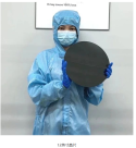
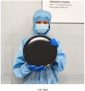
Semiconductor Industry Network learned that recently, Ningbo Hesheng New Materials Co., Ltd., a subsidiary of Hesheng Silicon Co., Ltd., successfully developed 12-inch (300mm) conductive silicon carbide (SiC) crystals and started research on cutting, grinding, polishing and other processing technologies. After years of dedicated research and in-depth research, Ningbo Hesheng New Materials has successfully overcome the core technical difficulties of the entire process from high-purity graphite purification, silicon carbide polycrystalline powder preparation to single crystal silicon carbide growth and substrate processing. In the past 2024, the company has made important breakthroughs in the field of silicon carbide materials, and 8-inch silicon carbide substrates have been mass-produced. This is an important milestone in the company's silicon carbide project research process, marking that Hesheng Silicon has reached the international advanced level in large-size silicon carbide crystal and wafer preparation technology. But Hesheng Silicon is not satisfied with this. In May 2025, it also made great progress in the preparation of larger-size ingots and substrates, and has broken through the 12-inch SiC crystal growth technology.


The successful development of 12-inch silicon carbide (SiC) crystals is of milestone significance in the development of the semiconductor industry. Wafers produced by large-size crystals mean that the number of chips per unit area can be greatly increased, which greatly reduces the material waste caused by the inability to fully utilize the edge area of the wafer, effectively reduces the manufacturing cost of power devices, and improves economic benefits. At the same time, SiC devices are widely used in high-efficiency industries such as new energy vehicles, photovoltaic power generation, and 5G communications, which are crucial to energy efficiency and volume optimization. Breakthroughs in large-size wafers will accelerate the upgrading of these industries.

