Chinese semiconductor thread II

tokenanalyst

Brigadier
Registered Member

Jingchi Electromechanical: Delivered the first 12-inch silicon carbide equipment in Hebei​


Hebei Jingchi Electromechanical Co., Ltd. (hereinafter referred to as "Jingchi Electromechanical") held a delivery ceremony for the first 12-inch resistance method high-purity silicon carbide crystal growth furnace in Hebei Province.

It is reported that the 12-inch resistance-based high-purity silicon carbide crystal growth furnace delivered by Jingchi Electromechanical this time adopts the resistive physical vapor transport (PVT) method. Through innovative structure and thermal field design, combined with advanced process control theory and automated control methods, it achieves uniform radial temperature and a wide range of precisely adjustable axial temperature gradients. This design enables the equipment to accurately control the process parameters during the crystal growth process and achieve highly intelligent operation. According to the news, the equipment can seamlessly "switch with one button" to produce 8-inch and 12-inch silicon carbide single crystals, greatly improving the flexibility and production efficiency of the equipment.

1747751288603.png


The successful delivery of the 12-inch resistance method high-purity silicon carbide crystal growth furnace not only sets a new milestone for Jingchi Electromechanical in the field of semiconductor material equipment manufacturing, but also provides strong support for the independent and controllable development of my country's semiconductor industry. In the future, Jingchi Electromechanical will continue to deepen the cooperation between industry, academia and research, strengthen independent innovation capabilities, continuously optimize product performance, and improve the efficiency of technology transformation. At the same time, the company will further expand its production scale to meet the global market demand for high-performance silicon carbide materials.

It is worth noting that as early as March this year, Jingchi Electromechanical successfully completed the 12-inch polycrystalline growth verification and achieved stable mass production of 8-inch and 12-inch silicon carbide single crystals on the same furnace, marking a new breakthrough in the domestic equipment in the technical breakthrough of large-size silicon carbide substrates. In January this year, the 8-inch silicon carbide resistive crystal growth furnace developed by Jingchi Electromechanical passed customer verification and officially started small-batch delivery. In addition, its independently developed "fully automatic silicon carbide corrosion cleaning equipment" was also successfully delivered to overseas customers.

Please, Log in or Register to view URLs content!
 

tokenanalyst

Brigadier
Registered Member

Epitaxial base put into production, GaN chips exceed 100 million, China Resources Microelectronics achieves success on two fronts.​


On May 16, Runxin Microelectronics (Dalian) Co., Ltd., a subsidiary of China Resources Microelectronics Power Devices Business Group, held the "GaN Billionth Chip Celebration and Epitaxial Production Base Opening Ceremony" at the Huangnichuan Intelligent Manufacturing Industrial Park in Dalian High-tech Zone. The event officially announced the completion and commissioning of its GaN epitaxial production base, and simultaneously celebrated the cumulative shipment of GaN chips exceeding 100 million.​

Epitaxial production base officially put into operation

According to official disclosure, the epitaxial production base took only nine months from project initiation to production start-up. The base has a total construction area of 6,238.38 square meters, and supporting ancillary facilities cover an area of 2,966.6 square meters. It focuses on the production of third-generation semiconductor gallium nitride epitaxial materials and electronic components.

The Vice President of China Resources Microelectronics, emphasized in his speech that this base is a key milestone in China Resources Microelectronics' layout of GaN production lines, marking the company's formation of full-chain technical capabilities from epitaxial material preparation to device process optimization. The Deputy Director of the Dalian High-tech Zone Management Committee, said that the base is a model of central-local cooperation and will help upgrade the regional semiconductor industry.

Cumulative shipments of GaN chips exceeded 100 million


Runxin Microelectronics' GaN chip shipments have exceeded 100 million, and its products are distributed in multiple market segments. In the field of consumer electronics, its products are widely used in PD fast charging chargers, such as Nothing CMF 65W, Esawat 65W and other brand products, which help devices achieve miniaturization and high efficiency with their high power density and low loss characteristics.

In the industrial field, Runxin Microelectronics' gallium nitride devices have entered the communication equipment, servo motor and high-end motor drive markets. For example, the Gushi 188W multi-port desktop charger uses its XG65T125HS1B device, which supports high-frequency switching and does not require a freewheeling diode, significantly improving system efficiency.


In addition, Runxin Microelectronics is accelerating the expansion of the new energy vehicle market, planning automotive-grade GaN products, and working with China Resources Microelectronics to promote the application of GaN in power management, battery systems, etc. The company has established cooperation with many leading customers in the industry, and its market brand influence has been greatly improved.

China Resources Microelectronics stated that it will continue to increase R&D investment in the future, promote collaborative innovation in the semiconductor industry chain, and help my country achieve a technological breakthrough in the high-end power device market.

Please, Log in or Register to view URLs content!
 

tokenanalyst

Brigadier
Registered Member

Drafts for comments on two standards, "GaN HEMT DHTOL, GaN HEMT epitaxial wafers on silicon substrates for power devices"​


Xiamen Sanan Integrated Circuit Co., Ltd. took the lead in drafting T/CASAS 057202X "GaN Power Device Switch Operation State Reliability Test Method under High Frequency Switch Application"

On April 29, 2025, the draft of T/CASAS 057-202X "Reliability Test Method for Switch Operation of GaN Power Devices under High Frequency Switching Applications" drafted by Xiamen Sanan Integrated Circuit Co., Ltd. and T/CASAS 060-202X "GaN HEMT Epitaxial Wafers on Silicon Substrates for Power Devices" drafted by Suzhou Jingzhan Semiconductor Co., Ltd. have been completed and officially solicited opinions from alliance members for one month. According to the Alliance Standardization Management Measures, the solicitation of opinions will start on April 29, 2025 and end on May 29, 2025.


T/CASAS 057—202X "Reliability test method for GaN power device switching operation status under high frequency switching application"
This document specifies the reliability test method for evaluating the switching operation status of GaN power devices in high-frequency switching applications (frequency ≥ 100kHz). It is used to characterize and evaluate the degradation and failure of GaN power devices under continuous switching stress to ensure their stable operation in typical application areas represented by fast charging adapters and to achieve improved overall system performance.
This document is applicable to the production R&D, characteristic characterization, mass production testing, reliability evaluation and application evaluation of GaN power devices. It can be applied to the following devices:
1) GaN enhancement mode (E-Mode) and depletion mode (D-Mode) discrete power electronic devices;
2) GaN power integrated devices and cascode GaN power devices;
3) Wafer-level and package-level products mentioned above.

T/CASAS 060—202X《GaN HEMT epitaxial wafers on silicon substrate for power devices》
This document specifies the classification and marking, requirements, test methods, inspection rules, marking, packaging, transportation and storage of GaN HEMT epitaxial wafers on silicon substrates for power devices.
This document applies to silicon substrate GaN HEMT epitaxial wafers for power devices. The products are mainly used to make power semiconductors and electronic devices.


Please, Log in or Register to view URLs content!
 

tokenanalyst

Brigadier
Registered Member

Focuslight Technology's Wafer-Level Lens Stacking (WLS) technology won the "Leading Enterprise Award" and "Process Pioneer Award" for outstanding cases of industrialization of micro-nano manufacturing technology​


Recently, Juguan Technology's wafer-level lens stacking (WLS) technology won the "Leading Enterprise Award" and "Process Pioneer Award" in the "2024-2025 Micro-Nano Manufacturing Technology Industrialization Outstanding Case Selection" organized by Suzhou Nano City and Shenzhen Micro-Nano Manufacturing Industry Promotion Association.

1747754089027.png

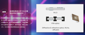
Juguang Technology's wafer-level lens stacking (WLS) technology uses semiconductor technology to mass-produce lenses on a whole glass wafer, and then press multiple lens wafers together and finally cut them into a single micro optical imaging lens. Its advantages are: 1. It can efficiently realize the miniaturization and high precision of micro-nano optical components and modules, and is easy to expand for mass production; 2. It can achieve micron-level precise stacking of optical wafers, and can integrate additional functions such as apertures, coatings, and spectral filters; 3. It can provide a reflow solution suitable for CSP sensors to ensure the stability and efficiency of optical products.

Please, Log in or Register to view URLs content!
 

tphuang

General
Staff member
Super Moderator
VIP Professional
Registered Member
we are totally moving forward toward 12-inch SiC in China


Epitaxial base put into production, GaN chips exceed 100 million, China Resources Microelectronics achieves success on two fronts.​


On May 16, Runxin Microelectronics (Dalian) Co., Ltd., a subsidiary of China Resources Microelectronics Power Devices Business Group, held the "GaN Billionth Chip Celebration and Epitaxial Production Base Opening Ceremony" at the Huangnichuan Intelligent Manufacturing Industrial Park in Dalian High-tech Zone. The event officially announced the completion and commissioning of its GaN epitaxial production base, and simultaneously celebrated the cumulative shipment of GaN chips exceeding 100 million.​

Epitaxial production base officially put into operation

According to official disclosure, the epitaxial production base took only nine months from project initiation to production start-up. The base has a total construction area of 6,238.38 square meters, and supporting ancillary facilities cover an area of 2,966.6 square meters. It focuses on the production of third-generation semiconductor gallium nitride epitaxial materials and electronic components.

The Vice President of China Resources Microelectronics, emphasized in his speech that this base is a key milestone in China Resources Microelectronics' layout of GaN production lines, marking the company's formation of full-chain technical capabilities from epitaxial material preparation to device process optimization. The Deputy Director of the Dalian High-tech Zone Management Committee, said that the base is a model of central-local cooperation and will help upgrade the regional semiconductor industry.

Cumulative shipments of GaN chips exceeded 100 million


Runxin Microelectronics' GaN chip shipments have exceeded 100 million, and its products are distributed in multiple market segments. In the field of consumer electronics, its products are widely used in PD fast charging chargers, such as Nothing CMF 65W, Esawat 65W and other brand products, which help devices achieve miniaturization and high efficiency with their high power density and low loss characteristics.

In the industrial field, Runxin Microelectronics' gallium nitride devices have entered the communication equipment, servo motor and high-end motor drive markets. For example, the Gushi 188W multi-port desktop charger uses its XG65T125HS1B device, which supports high-frequency switching and does not require a freewheeling diode, significantly improving system efficiency.


In addition, Runxin Microelectronics is accelerating the expansion of the new energy vehicle market, planning automotive-grade GaN products, and working with China Resources Microelectronics to promote the application of GaN in power management, battery systems, etc. The company has established cooperation with many leading customers in the industry, and its market brand influence has been greatly improved.

China Resources Microelectronics stated that it will continue to increase R&D investment in the future, promote collaborative innovation in the semiconductor industry chain, and help my country achieve a technological breakthrough in the high-end power device market.

Please, Log in or Register to view URLs content!
yeah, I saw this. China should dominate GaN production and put the Western chipmakers out of business here. How are they still producing stuff with reduced Gallium export? This is the question I have.
Please, Log in or Register to view URLs content!


Finally domestic 4inch AlN single crystal substrate wafer. They are about two years behind Crystal IS.
Please, Log in or Register to view URLs content!

AlN is also much better substrate material than S or SiC for GaN epitaxy. I see huge Chinese progress in Ga2O3, good progress in diamond and rapid catch-up in AlN
yes, this is very important.

btw, you are right on Ga2O3, especially with Garen semi. they are doing 8-inch wafers and there seems to be customers lining up
 

tokenanalyst

Brigadier
Registered Member
yeah, I saw this. China should dominate GaN production and put the Western chipmakers out of business here. How are they still producing stuff with reduced Gallium export? This is the question I have.
China export controls of Gallium is for US and the Holland, i think, mainly because their own export controls to China, so pretty much like chip making tools there are many ways that Chinese Gallium exports can reach those countries, because supply chains are complex.

1747755145630.png

Take it with truck load of salt because I don't know how reliable this source is.

Please, Log in or Register to view URLs content!
 

tphuang

General
Staff member
Super Moderator
VIP Professional
Registered Member
China export controls of Gallium is for US and the Holland, i think, mainly because their own export controls to China, so pretty much like chip making tools there are many ways that Chinese Gallium exports can reach those countries, because supply chains are complex.

View attachment 152631

Take it with truck load of salt because I don't know how reliable this source is.

Please, Log in or Register to view URLs content!
export control is global. The ban is only to US. I've spoke about this several times before. Transshipment is a huge issue right now, that's why they are looking to tighten the licensing process.
 

ZeEa5KPul

Colonel
Registered Member
export control is global. The ban is only to US. I've spoke about this several times before. Transshipment is a huge issue right now, that's why they are looking to tighten the licensing process.
Strange that they didn't anticipate this since China is the world leader in transshipment. They could have just looked at their own tricks.
 

tphuang

General
Staff member
Super Moderator
VIP Professional
Registered Member

I wrote about Kirin 8020 here and how it compares to 9020 and 9020A. I think it is kind of like intel chips where there are multiple bins. 9020 is likely the best bin, followed by 9020A, followed by 8020. Maybe they can create another bin with reduced cores for even lower end phones to fully utilize 7nm capacity.
 
Top