Chinese semiconductor thread II

sunnymaxi

Major
Registered Member
It would be too naive for Xiaomi to bet such a big investment on a promise by a US company.

Maybe there is also some assurance from China that if something happens Qualcomm would be kicked out and they already informed US accordingly....this could work (for a while) with the average US administration, but with Trump it is like flipping the coin. Trump can very well block TSMC and if China retaliates block also Mediatek to sell in China....this would escalate quickly and ugly.

The key point is that Xiaomi relies on an advanced 4nm N4P process node, China will not have something similar for a while. Instead Huawei relies on a localized 7nm node, already in volume production, that's a totally different scenario.

At best with the Qualcomm agreement they have bought some free months, following Huawei example, they should use these precious (and very expensive) months to stockpile furiously a couple of years of production: buy all that TSMC can produce....and then when the US hammer will come, sell for another 2 years, and then switch on what will be local SOTA around 2027.

They have started from zero and now they have a world-class 2500 people semiconductor team with proven knowledge and experience on a SOTA chip: even if they just recover the
Please, Log in or Register to view URLs content!
that would be already a huge win.

An interesting technical note. Xiaomi
Please, Log in or Register to view URLs content!
in its new XRING chip. That would be a first for UNISOC at such advanced process node and SOTA chip.


Wolfspeed is market leader with more than
Please, Log in or Register to view URLs content!


View attachment 152667

US cannot just let Wolfspeed go.

Bankrupt protection is not the end of the road, they just want to restructure the debt with creditors....but I guess someone will buy them and keep them running.

US can easily force automotive manufacturers that want to sell in US to stop using China SiC (actually this is a very predictable move) and Wolfspeed will reborn into a second life.

My bet is to wait a bit for things to calm down and then even buy
Please, Log in or Register to view URLs content!
:)
This is first casualty of China's semi industry growth. more to come in coming years.

Wolfspeed may not go bankrupt but revenue will take a huge hit. that is enough for us.
 

tphuang

General
Staff member
Super Moderator
VIP Professional
Registered Member
It would be too naive for Xiaomi to bet such a big investment on a promise by a US company.

Maybe there is also some assurance from China that if something happens Qualcomm would be kicked out and they already informed US accordingly....this could work (for a while) with the average US administration, but with Trump it is like flipping the coin. Trump can very well block TSMC and if China retaliates block also Mediatek to sell in China....this would escalate quickly and ugly.

The key point is that Xiaomi relies on an advanced 4nm N4P process node, China will not have something similar for a while. Instead Huawei relies on a localized 7nm node, already in volume production, that's a totally different scenario.

At best with the Qualcomm agreement they have bought some free months, following Huawei example, they should use these precious (and very expensive) months to stockpile furiously a couple of years of production: buy all that TSMC can produce....and then when the US hammer will come, sell for another 2 years, and then switch on what will be local SOTA around 2027.

They have started from zero and now they have a world-class 2500 people semiconductor team with proven knowledge and experience on a SOTA chip: even if they just recover the
Please, Log in or Register to view URLs content!
that would be already a huge win.

An interesting technical note. Xiaomi
Please, Log in or Register to view URLs content!
in its new XRING chip. That would be a first for UNISOC at such advanced process node and SOTA chip.
They really don't need this to last more than a couple of years really. They can buy 2 years of supply from TSMC like what Huawei did.

You guys are over thinking it. As long as QCOM's share on the premium end doesn't drop too much, there is pressure on QCOM from Chinese customers to not complain to US govt. The current US admin attention is mostly on Huawei and AI chips.

Wolfspeed is market leader with more than
Please, Log in or Register to view URLs content!


View attachment 152667

US cannot just let Wolfspeed go.

Bankrupt protection is not the end of the road, they just want to restructure the debt with creditors....but I guess someone will buy them and keep them running.

US can easily force automotive manufacturers that want to sell in US to stop using China SiC (actually this is a very predictable move) and Wolfspeed will reborn into a second life.

My bet is to wait a bit for things to calm down and then even buy
Please, Log in or Register to view URLs content!
:)
You are looking at 2024 data. This will change very fast, because SiC adoption has really picked up in China this year. Wolfspeed bet on all this increased demand to use their substrate, which is clearly not happening.
Probably the bigger issue is not even market share but that price has dropped so much.
 

tokenanalyst

Brigadier
Registered Member

The first equipment of Hefei Xingu Microelectronics GaAs wafer manufacturing line was moved in​


According to the official microblog of Hefei XinGu Microelectronics, on May 19, the Hefei XinGu Microelectronics GaAs wafer manufacturing line project reached an important milestone - the first core equipment, the high-temperature ion implanter, was successfully moved in. This move marks that the production line has officially entered the equipment installation and commissioning stage. All equipment is scheduled to be moved in by the end of May, laying a solid foundation for the subsequent line operation and production.
It is reported that the construction of the production line will start in 2023 and is planned to be a 6-inch gallium arsenide wafer manufacturing line. The products are widely used in wireless communications, radar, electronic countermeasures, guidance and other fields. After the project is put into production, it will further enrich the company's product line, enhance Core Valley's competitiveness in the semiconductor field, and accelerate the breakthrough and application of domestic semiconductor manufacturing technology. At the same time, Core Valley will also achieve full industrial chain connection from chip design, wafer manufacturing, packaging and testing, microwave component design and production, and complete the transformation into an IDM company.

1747838509982.png

Please, Log in or Register to view URLs content!
 

tokenanalyst

Brigadier
Registered Member

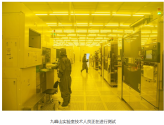
A number of high-growth integrated circuit companies have set up R&D institutions and production lines in Optics Valley​


In the past two months, many integrated circuit industry chain companies such as Sunshu Technology, Cixin Technology, and Junyuan Electronics have signed contracts to settle in Optics Valley and set up R&D institutions and production lines. These companies have been established for an average of less than 6 years and have grown into high-growth companies in the sub-sectors of chip design, manufacturing, packaging and testing, equipment and materials.

Junyuan Electronics will build the company's first high-end chip R&D and production base in Central China, and the production line is expected to be put into use next month; Quanxin Intelligent Manufacturing will build a domestic manufacturing EDA project in Optics Valley, and its new office located in East Lake Science City has been put into use.

In the past year, Optics Valley has signed about 30 new projects with a value of more than 100 million yuan around the storage semiconductor industry chain, covering core equipment, components, key raw materials, EDA software, wafer manufacturing, packaging and testing, modules and other fields. In the field of compound semiconductors, relying on the "research-test-production" ecological system of Jiufengshan Laboratory, 30 innovative companies have settled in Optics Valley, and another 18 are in the process of transformation.

From investing in the establishment of my country's first memory wafer factory in 2005, to building the National Memory Base Project in 2016, to building the Jiufengshan Laboratory in 2021 to create the second growth curve in the optoelectronic information field, in 20 years, Optics Valley has built a "3+2" integrated circuit industry system dominated by storage semiconductors, compound semiconductors and three-dimensional integration, and featuring advanced packaging and silicon photonic integrated circuits. In 2024, the scale of the integrated circuit industry will exceed 80 billion yuan.

At present, a number of major integrated circuit projects in Optics Valley are being accelerated: the main structure of the Pioneer Rare Materials Project was fully topped off not long ago, and masonry painting, electromechanical installation and outdoor construction are being carried out simultaneously. Factory decoration will begin next month; the Changfei Advanced Wuhan Base Project has also entered the final equipment debugging stage and is expected to achieve mass production by the end of the month. After reaching full production, it will effectively alleviate the domestic demand for high-end chips for new energy vehicles.

1747838872713.png

In addition, Optics Valley is planning to build a 7-square-kilometer memory industry innovation block and a 14-square-kilometer compound semiconductor industry innovation block, provide 1 million square meters of high-standard factory buildings each year, establish the Optics Valley High-Quality Development Fund, and add a new parent-child fund cluster covering the entire life cycle of angel funds, venture capital, mergers and acquisitions, with a focus on investing in optoelectronic information industries such as integrated circuits.

Please, Log in or Register to view URLs content!
 

tokenanalyst

Brigadier
Registered Member

Total investment of 5.5 billion! Silicon carbide industrial park project landed in Inner Mongolia​


According to the Tongliao CPPCC, Kulun Banner, Tongliao City, Inner Mongolia Autonomous Region recently welcomed a major investment project - a silicon carbide industrial park project with a total investment of 5.5 billion yuan.

The project has a total investment of 5.5 billion yuan, covers an area of 270 mu, and is constructed in three phases. It is planned to reach full production within three years. Among them, the first phase will invest 500 million yuan to build a semiconductor-grade silicon carbide powder material (electronic-grade silicon micropowder) processing plant with an annual output of 150,000 tons; the second phase will invest 2.5 billion yuan to build a carbon-carbon composite material processing plant with an annual output of 500,000 square meters; the third phase will invest 2.5 billion yuan to build a carbon-carbon composite brake disc processing plant with an annual output of 300,000 sets (pieces).
The project investor, Zhongke Composites (Jilin) Technology Co., Ltd., was established on June 4, 2021 with a registered capital of RMB 50 million. It is located in the Shengkailun Double Innovation Base in Yushu City, Changchun City, Jilin Province. The company's business scope covers new material technology research and development, high-performance fiber and composite material manufacturing, and carbon fiber recycling technology research and development.

Please, Log in or Register to view URLs content!
 

tokenanalyst

Brigadier
Registered Member

Fast and Accurate EUVL Thick-Mask Model Based on Multi-Channel Attention Network​

Abstract:​

Simulation of thick-mask effects is an important task in computational lithography within extreme ultraviolet (EUV) waveband. This paper proposes a fast and accurate learning-based thick-mask model dubbed multi-channel block attention network (MCBA-Net) to solve this problem for EUV lithography. The proposed MCBA-Net introduces geometric feature attention module and structural feature attention module to improve the computation accuracy of thick-mask diffraction near field. During the training process, the proposed attention modules can effectively learn the impact of the three-dimensional mask diffraction behavior. In addition, the multi-channel network architecture is used to simultaneously synthesize the thick-mask diffraction matrices under different polarization states, and the coupling between different diffraction matrices is addressed. Numerical experiments show that the proposed model improves the computational efficiency by more than 20-fold over the rigorous simulator, and reduces the prediction error by 25%~50% compared with the state-of-the-art deep learning models. In addition, the generalization ability of the proposed method is proved using a complex testing pattern.​

Please, Log in or Register to view URLs content!
 

tokenanalyst

Brigadier
Registered Member

DPFEE-Net: Enhancing Wafer Defect Classification Through Dual-Path Neural Architecture​

Abstract:​

Wafer defect detection and classification are essential for ensuring the quality of semiconductor wafers, optimizing production efficiency. However, existing methods often fail to process shallow and deep feature information concurrently, restricting their capacity to utilize multi-level features for accurate classification. To overcome this limitation, this paper introduces a novel dual-path architecture, DPFEE-Net, which integrates PeleeNet’s dense connection structure and multi-channel feature fusion techniques with the deep feature extraction capabilities of Convolutional Neural Networks (CNNs). By combining these two approaches, DPFEE-Net effectively captures both shallow and deep features, enhancing the detection of critical wafer surface defect patterns. Additionally, squeeze-and-excitation (SE) attention mechanism is incorporated, enabling the model to prioritize defect-prone areas in images, further improving classification accuracy. Experimental results demonstrate that DPFEE-Net achieves a remarkable average accuracy of 96.8% on the WM-811K dataset, surpassing existing methods such as WM-PeleeNet, WDD-SCA and MobileNetV2. Moreover, the model delivers superior detection performance with reduced computational complexity and parameter requirements, making it highly suitable for practical deployment in production environments.​

Please, Log in or Register to view URLs content!
 

tokenanalyst

Brigadier
Registered Member

RA-UNet: A New Deep Learning Segmentation Method for Semiconductor Wafer Defect Analysis on Fine-Grained Scanning Electron Microscope (SEM) Images​

Abstract:​

In the rapidly evolving field of semiconductor manufacturing, the escalating complexity of integrated circuits poses significant challenges in identifying and analyzing defects, crucial for maintaining high wafer yield. Traditional approaches are hindered by the intricate nature of defect morphology and the scarcity of high-quality scanning electron microscope (SEM) data, essential for effective algorithm training. In this study, we propose RA-UNet for fine-grained SEM defect segmentation. RA-UNet adopts a U-shaped architecture that leverages residual networks for defect feature extraction, and introduces a residual architecture and a novel attention module to enhance the network’s focus on defects. To validate the effectiveness of the proposed model, we meticulously gathered and labeled a real SEM data set from a semiconductor manufacturing factory. The results demonstrate that RA-UNet outperforms existing methods in semiconductor defect segmentation, achieving an Intersection over Union (IoU) score of 71.92%. These findings highlight its potential as an effective tool for semiconductor defect analysis.​

Please, Log in or Register to view URLs content!
 

tokenanalyst

Brigadier
Registered Member
Shanghai Institute of Optics and Fine Mechanics has made new progress in the research of laser high-precision polishing mechanism and process

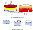
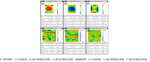
Recently, the team led by Wei Chaoyang, a researcher , has made new progress in the research of laser high-precision polishing mechanism and process. The research revealed the mechanism of shape deterioration after laser polishing, and proposed a laser double-sided polishing process to improve processing accuracy. The relevant research results were published in Optics & Laser Technology under the title " Formation mechanism and suppression method of surface deterioration in CO2 laser polishing for fused silica" .

With the development of modern optical technology, the UV laser-induced damage problem of fused quartz components has seriously restricted the development of high-power laser systems. At present, laser polishing is expected to achieve the processing of high-threshold fused quartz components due to its technical advantages of non-contact, no processing auxiliary materials and flexible processing. However, laser polishing will produce uneven scanning tracks due to the influence of thermal stress, which will seriously deteriorate the surface quality and reduce the performance and life of the component.

To this end, the researchers established a multi-physics field coupling model that takes into account solid heat transfer, fluid flow and structural mechanics, revealing the formation mechanism of the scanning trajectory. Studies have shown that the synergistic effect of recoil pressure and Marangoni effect induces molten pool oscillation and forms a scanning trajectory. By optimizing the polishing time, the surface roughness can be greatly reduced while avoiding the generation of scanning trajectories. In addition, a laser double-sided polishing method is proposed to address the uncontrollable scanning trajectory caused by power fluctuations of industrial lasers. Experiments have confirmed that laser double-sided polishing can reduce the RMS value of the surface shape from 0.433λ to 0.194λ , improve the roughness from 0.371 nm to 0.270 nm , and increase the 0% probability damage threshold from 19.4 J/cm² to 21.2 J/cm² . This study not only explains the multi-field coupling mechanism of surface shape deterioration in laser polishing, but also provides a process paradigm for the controllable manufacturing of fused quartz components with sub-nanometer precision and high damage threshold.

1747844343154.png1747844375866.png

Please, Log in or Register to view URLs content!
 

Topazchen

Junior Member
Registered Member
It would be too naive for Xiaomi to bet such a big investment on a promise by a US company.

Maybe there is also some assurance from China that if something happens Qualcomm would be kicked out and they already informed US accordingly....this could work (for a while) with the average US administration, but with Trump it is like flipping the coin. Trump can very well block TSMC and if China retaliates block also Mediatek to sell in China....this would escalate quickly and ugly.

The key point is that Xiaomi relies on an advanced 4nm N4P process node, China will not have something similar for a while. Instead Huawei relies on a localized 7nm node, already in volume production, that's a totally different scenario.

At best with the Qualcomm agreement they have bought some free months, following Huawei example, they should use these precious (and very expensive) months to stockpile furiously a couple of years of production: buy all that TSMC can produce....and then when the US hammer will come, sell for another 2 years, and then switch on what will be local SOTA around 2027.

They have started from zero and now they have a world-class 2500 people semiconductor team with proven knowledge and experience on a SOTA chip: even if they just recover the
Please, Log in or Register to view URLs content!
that would be already a huge win.

An interesting technical note. Xiaomi
Please, Log in or Register to view URLs content!
in its new XRING chip. That would be a first for UNISOC at such advanced process node and SOTA chip.


Wolfspeed is market leader with more than
Please, Log in or Register to view URLs content!


View attachment 152667

US cannot just let Wolfspeed go.

Bankrupt protection is not the end of the road, they just want to restructure the debt with creditors....but I guess someone will buy them and keep them running.

US can easily force automotive manufacturers that want to sell in US to stop using China SiC (actually this is a very predictable move) and Wolfspeed will reborn into a second life.

My bet is to wait a bit for things to calm down and then even buy
Please, Log in or Register to view URLs content!
:)
There is a real need to reduce reliance on American platform and component suppliers like Google and Qualcomm, respectively.

The fact that the U.S. can cripple a major Chinese tech firm by denying access to essential platforms or components represents an unacceptable vulnerability.

Well done Xiaomi
 
Top