Chinese semiconductor thread II

tokenanalyst

Brigadier
Registered Member

Kezhuo Semiconductor Completes RMB 70 Million Series A Financing​


Recently, Kezhuo Semiconductor completed its first round of financing after commercialization, raising 70 million yuan.
Founded in 2016 and based in Dongguan, the company focuses on the research, development, production and sales of high-end semiconductor packaging equipment. In 2018, it took the lead in successfully developing the country's first 12-inch fully automatic wafer cutting machine (Wafer Saw). After 8 years of research and development, 8 iterations and more than 4 years of actual production line verification, it has formed a series of equipment including wafer cutting machines (Wafer Saw), IC finished product cutting (Package Saw), finished product cutting high-speed sorting machines (JigSaw), FC die bonding machines (Flip Chip), etc. It has nearly 20 packaging customers, with an accuracy of 2 microns, stable and reliable, and is at the leading level in China.

1746639535764.png

Please, Log in or Register to view URLs content!
 

tokenanalyst

Brigadier
Registered Member

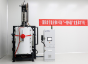
Hangzhou Fuga Gallium Industry's "One-click Crystal Growth" Equipment Passed Customer On-site Acceptance.​

Recently, the gallium oxide EFG method equipment independently developed by Hangzhou Fuga Gallium Technology Co., Ltd. completed on-site acceptance and went offline smoothly. This equipment with the "one-click crystal growth" function realizes intelligent control of crystal growth, marking a major breakthrough in gallium oxide single crystal preparation technology and laying a solid foundation for the large-scale production of high-performance semiconductor materials.
1746649337422.png
Gallium oxide (Ga₂O₃), as a core material of power devices with great potential, has long been constrained by problems such as high-temperature volatilization decomposition, anisotropy and thermal field asymmetry, and its industrialization process has been slow. Fuga Gallium Industry adheres to the "dual-wheel drive" strategy of process and equipment. By optimizing the core links of the EFG growth process, deeply embedding the technology related to crystal growth habits into the equipment, and integrating machine learning technology, it has successfully realized the "unmanned driving" mode of gallium oxide single crystal growth. This technology effectively reduces the dependence on manual experience and significantly improves the efficiency and quality of crystal production. It passed the industry expert evaluation and certification in December 2024 (Fugia Gallium Industry's "one-key crystal growth" technology passed the expert evaluation, and the fully automatic crystal growth equipment helped the gallium oxide industry take off).

The successful passing of the customer's on-site acceptance not only verifies the reliability of the equipment technology, but also indicates that the "one-click crystal growth" technology has been recognized by the market. Fuga Gallium will take the official launch of the equipment as a new starting point, continue to promote collaborative innovation in technology and equipment, accelerate the pace of industrialization of gallium oxide materials, and help my country achieve a new leap in the field of high-performance semiconductors.


Please, Log in or Register to view URLs content!
 

tokenanalyst

Brigadier
Registered Member

Fulat completes Pre-A round of financing to accelerate the localization of wet cleaning equipment​


Recently, semiconductor wet process equipment supplier Flat announced that it has completed tens of millions of yuan in Pre-A round of financing.

This round of investment was led by well-known institutions such as Zijin New Capital, Jingkai Juzhi, and Dongfang Industrial Finance, and Kuangben Capital served as the exclusive financing advisor.

This round of financing will help the company deepen domestic research and development in the field of wet cleaning equipment, enhance its large-scale mass production and delivery capabilities, and further promote the independent and controllable development of China's semiconductor industry.​

1746649629003.png
1746649722203.png

Please, Log in or Register to view URLs content!
 

tokenanalyst

Brigadier
Registered Member

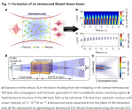
Efficient generation of Bessel-Gauss attosecond pulse trains via nonadiabatic phase-matched high-order harmonics.​

Abstract​

Generating Bessel-Gauss beams in the extreme ultraviolet (EUV) with attosecond pulse durations poses a significant challenge due to the limitations of conventional transmission optical components. Here, we propose a novel approach to produce such beams by inducing an annular EUV source through high-order harmonic generation (HHG) under nonadiabatic phase-matching conditions. The resulting light pulse maintains temporal coherence and manifests attosecond pulse trains as confirmed by the reconstruction of attosecond beating by interference of two-photon transitions (RABBIT) measurements. Macroscopic HHG calculations reproduce the measured spatiotemporal structures, demonstrating the plasma-induced spatial modulation on the formation of an annular source. Propagation simulations further confirm the feasibility of this approach for generating attosecond Bessel-Gauss beams, presenting exciting prospects for various applications in EUV photonics and attosecond science.

1746649950234.png

Please, Log in or Register to view URLs content!
 

Michael90

Junior Member
Registered Member
Looks like majority of the analog technology for New energy vehicle charging station is foreign.

These are all old technology, there's no excuse for not able to be self sufficient on this.

China have a lot of room to improve on this. Many industrial products still using tons of US analog chips.

Please, Log in or Register to view URLs content!

1)The isolation amplifier is from Broadcom, model ACPL-C790, and is used for input current sensing isolation.

2)ON Semiconductor MC33274A 4-op amp is used for current signal amplification.

3)Three voltage regulator chips are used to power the isolation amplifier. The voltage regulator chip comes from STMicroelectronics, model LD1117S50TR, with an input voltage of 15V, an output voltage of 5V, an output current of 800mA, and is packaged in SOT-223.

4)The auxiliary power supply main control chip comes from STMicroelectronics, model UC2845B, which is a high-performance current mode controller in SO8 package.

5)The driver chip comes from Microchip Technology, model MIC4428, which is a dual-channel low-side driver with an output current of 1.5A. It uses a SOIC-8 package and is used to drive the auxiliary power transformer.

6)Close-up of STMicroelectronics' LD1117S50TR voltage regulator chip.

7)ON Semiconductor MC33274A 4 op amp for voltage sampling

8)The PFC (Power Factor Correction)controller comes from Texas Instruments, model TMS320F2808PZA. The chip integrates a C2000 32-bit MCU with a main frequency of 100MHz, built-in 128KB FLASH, supports linkage calculations, has fast interrupt response and processing, and uses LQFP100 packaging.

9) On Semi , Close-up of the 1.8V voltage regulator chip that powers the controller core.

10)ON Semiconductor MC33274A op amp is used for signal acquisition and amplification

11)STMicroelectronics LM239 quad voltage comparator is used for signal processing.

12)Close-up of the ON Semiconductor LM293 dual voltage comparator, which comes in a SOIC8 package and has five in total.

13)The step-down chip comes from Texas Instruments, model TPS5410, supports 36V input voltage, output current of 1A, internally integrated switching tube, and uses SOIC-8 package.
They are waiting for the US to ban them, when they have no choice than to turn to new alternatives. Lol So you can only hope Trump bans them from even this, that's what will get things changing
 

Michael90

Junior Member
Registered Member
Now they want to embed tracking and a kill switch into Nvidia chips.


Please, Log in or Register to view URLs content!
Seems no more Nvidia chips for Chinese companies from now on, not even smuggling will help anymore. Its not worth the money and time spent on it only to lose everything. They will have to learn to deal without Nvidia it seems. Tough times ahead.
 

huemens

Junior Member
Registered Member
Seems no more Nvidia chips for Chinese companies from now on, not even smuggling will help anymore. Its not worth the money and time spent on it only to lose everything. They will have to learn to deal without Nvidia it seems. Tough times ahead.
If it gets completely cut off that would be actually a good thing for China because it would accelerate adoption of domestic solutions. But those who want to smuggle will continue to do so. Even if this law comes to pass, whatever measures Nvdia implement would likely be minimal and easy to defeat and just enough for them to claim plausible deniability. Even now Nvidia would have fairly good idea of how much gets smuggled and through which countries. They don't need a tracker for that, but they continue to sell because they could claim plausible deniability.

Also there's some indication Trump may allow Nvidia to sell H20 after all. The Korean guy tweeted that Nvdia has still not asked to stop the manufacture of HBM's used in H20. He says based on that some industry sources believe Nvidia will get a permit for H20 soon. Or it may just be a rumor started by someone to pump Nvidia stock.

Either way, even if China can get Nvidia chips, the best thing for China would be to to move on to completely domestic solutions as soon as possible.
 

tokenanalyst

Brigadier
Registered Member

Han's Semiconductor achieves three new breakthroughs in 8/12-inch SiC substrate laser lift-off​


Currently, there is great pressure on the price of silicon carbide substrates to drop, and cost reduction is urgently needed. Traditional cutting processes generally rely on traditional multi-wire cutting technology, but this process is inefficient and has material loss, making it difficult to meet the processing needs of 6-8 inch large-size silicon carbide ingots, especially in the preparation of 12-inch optical waveguide silicon carbide lenses.
In order to solve the problem of mass production of laser lift-off technology, Han's Semiconductor has solved the problem with three breakthrough technologies:
● Fully compatible with low-resistance ingots: Breaking through the bottleneck of laser processing of low-resistivity ingots and achieving full coverage of conductive substrate resistivity requirements;
● Grinding wheel loss reduced by 40%+: LaserMesh™ interface technology is used to accurately control the peeling surface morphology (roughness ≤ 2μm, TTV < 10μm), combined with the interface softening process, which greatly reduces the subsequent thinning cost ;
● 12-inch mass production breakthrough: The world's first to achieve mass production of 12-inch conductive/semi-insulating crystal ingots by laser peeling, pushing large-size substrates into the "low cost, high yield" era, and laying the foundation for cost reduction of optoelectronics and radio frequency devices.​
To learn more about Han's Semiconductor's silicon carbide substrate laser stripping technology, please attend the "Electric Transportation & Digital Energy SiC Technology Application and Supply Chain Upgrade Conference" held by "Experts Talk about Three and a Half Generations" at the Shanghai Jinjiang Tomson InterContinental Hotel on May 15. At that time, Wu Lijie, general manager of the product line of Han's Semiconductor , will attend and give a speech on the topic of "Sharing the latest technological achievements in laser stripping technology in the preparation of 8/12 inch SiC substrates".

Please, Log in or Register to view URLs content!
 
Top