You are using an out of date browser. It may not display this or other websites correctly.
You should upgrade or use an alternative browser.
You should upgrade or use an alternative browser.
Chinese semiconductor thread II
- Thread starter vincent
- Start date
Having revenue cut down to single digits from double digits from one of the biggest market with huge growth potential in a very short amount of time, is not good, to say the least, when the hype is over and will be over, these huge markets are life saviors.
It is indeed not a good thing for Nvidia to lose the Chinese market, but it also doesn't contradict the fact that Nvidia is more than fine. Their were strong, demand continues to grow, etc, etc. The US market alone is large enough to support big players too, not even counting the rest of the world. There is hype, but it's not all just hype.
They could be doing even better, but they are still doing quite well. In a decade's time that might change, but nobody has a crystal ball.
please read the thread from the beginningright now China is getting by with lithography machines imported before sanctions hit. But what about the future. How can China move forward without imports from ASML?
please read the last 10 pages of this thread. you will get your answer. thanksright now China is getting by with lithography machines imported before sanctions hit. But what about the future. How can China move forward without imports from ASML?
China Wafer Bonding equipment industry
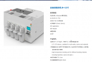
(1) Xinrui Technology
As a technological innovation enterprise, Xinrui Technology has been focusing on the research and development and innovation of semiconductor wafer bonding equipment. After more than ten years of research and development, its product applications cover all fields of semiconductors, and its process capabilities cover 2-12 inches. It is a temporary bonding equipment. , permanent bonding overall solution provider. Currently, nearly a hundred units of bonding equipment for compound semiconductors have been provided, and 12-inch temporary bonding and debonding equipment for 2.5D/3D packaging will be launched in 2023.
(2) Huazhuo Jingke
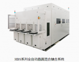
Wafer-level bonding equipment refers to the high-precision alignment and bonding of two wafers, and the use of external energy to react the atoms at the bonding interface to form a covalent bond and combine them into one, so that the bonding interface between the two wafers reaches Specific bonding strength, a device that realizes the integration of functional modules between two wafers.
Wafer-level bonding equipment integrates a variety of functional units and implements a complete process of wafer activation, cleaning, alignment, pre-bonding and verification within the equipment.
The company's wafer-level bonding equipment adopts wafer face-to-face alignment, which can adapt to more types of wafers made of base materials. By using precision control technology and pattern analysis algorithms, the wafer alignment accuracy reaches below 150nm, meeting the requirements of It meets process requirements such as wafer-level hybrid bonding and low-temperature bonding, and can conduct real-time online inspection of pre-bonded wafers and feed the results back to the control system, thereby improving bonding yield. The company can provide technology development services and products according to customers' customized needs, and assist customers in applying products to the manufacturing of CIS, 3D memory chips, MEMS and other devices.
(3) Tuojing Technology

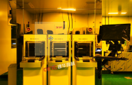
Figure 13: Models of wafer bonding equipment under development related to Tuojing’s public information
(4) Sanhe Jianhua Hi-Tech
Jianhua Hi-Tech Co., Ltd. was established in 2003 and is affiliated to the 45th Research Institute of China Electronics Technology Group Corporation. The company is located at No. 253 Haiyou Street, East Yanjiao Economic and Technological Development Zone, Beijing. The company currently has more than 60 technical personnel of various types and 30 with senior technical titles. Jianhua Hi-Tech Co., Ltd. aims to become "China's leader in semiconductor manufacturing equipment" and is committed to the research, development and manufacturing of semiconductor component material processing and chip manufacturing and testing special equipment. It strives to build high-precision machinery, optics, and equipment in North China. Electrical components manufacturing center.
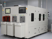
The equipment is mainly used for automatic alignment and wafer level temporary bonding process mainly suitable for 8 "and 12 substrates. Automatic manipulator feeding and unloading, process continuous processing, automatic operation. This product is easy to operate, high stability, good repeatability, and has a high cost performance, can be widely used in scientific research and production
(5) Bona Semiconductor
(1) Xinrui Technology
As a technological innovation enterprise, Xinrui Technology has been focusing on the research and development and innovation of semiconductor wafer bonding equipment. After more than ten years of research and development, its product applications cover all fields of semiconductors, and its process capabilities cover 2-12 inches. It is a temporary bonding equipment. , permanent bonding overall solution provider. Currently, nearly a hundred units of bonding equipment for compound semiconductors have been provided, and 12-inch temporary bonding and debonding equipment for 2.5D/3D packaging will be launched in 2023.

(2) Huazhuo Jingke
Wafer-level bonding equipment refers to the high-precision alignment and bonding of two wafers, and the use of external energy to react the atoms at the bonding interface to form a covalent bond and combine them into one, so that the bonding interface between the two wafers reaches Specific bonding strength, a device that realizes the integration of functional modules between two wafers.
Wafer-level bonding equipment integrates a variety of functional units and implements a complete process of wafer activation, cleaning, alignment, pre-bonding and verification within the equipment.
The company's wafer-level bonding equipment adopts wafer face-to-face alignment, which can adapt to more types of wafers made of base materials. By using precision control technology and pattern analysis algorithms, the wafer alignment accuracy reaches below 150nm, meeting the requirements of It meets process requirements such as wafer-level hybrid bonding and low-temperature bonding, and can conduct real-time online inspection of pre-bonded wafers and feed the results back to the control system, thereby improving bonding yield. The company can provide technology development services and products according to customers' customized needs, and assist customers in applying products to the manufacturing of CIS, 3D memory chips, MEMS and other devices.

(3) Tuojing Technology
In terms of advanced packaging, the company has actively entered the cutting-edge technology field of high-end semiconductor equipment and developed a series of hybrid bonding equipment for wafer-level three-dimensional integration. At the same time, the equipment is also compatible with fusion bonding. ). The company's hybrid bonding series products include Wafer to Wafer Bonding products and Die to Wafer Bonding Preparation and Activation products, which can achieve direct or inter-layer based Bonding process, complex room temperature covalent bonding process. According to public information, Tuojing is currently developing wafer bonding equipment, mainly hybrid bonding equipment, and its first Dione 300 model is currently being verified by customers.

Figure 13: Models of wafer bonding equipment under development related to Tuojing’s public information
(4) Sanhe Jianhua Hi-Tech
Jianhua Hi-Tech Co., Ltd. was established in 2003 and is affiliated to the 45th Research Institute of China Electronics Technology Group Corporation. The company is located at No. 253 Haiyou Street, East Yanjiao Economic and Technological Development Zone, Beijing. The company currently has more than 60 technical personnel of various types and 30 with senior technical titles. Jianhua Hi-Tech Co., Ltd. aims to become "China's leader in semiconductor manufacturing equipment" and is committed to the research, development and manufacturing of semiconductor component material processing and chip manufacturing and testing special equipment. It strives to build high-precision machinery, optics, and equipment in North China. Electrical components manufacturing center.
The equipment is mainly used for automatic alignment and wafer level temporary bonding process mainly suitable for 8 "and 12 substrates. Automatic manipulator feeding and unloading, process continuous processing, automatic operation. This product is easy to operate, high stability, good repeatability, and has a high cost performance, can be widely used in scientific research and production

(5) Bona Semiconductor
Shanghai Bona Microelectronics Equipment Co., Ltd. is a high-end equipment manufacturer integrating mechanical design, electrical research, software development, and precision manufacturing. It currently develops and produces core production equipment for the three major industries of advanced packaging, display, and semiconductor wafers. . The company is headquartered in Lingang Integrated Circuit Industrial Park, Shanghai Free Trade Zone, and has set up the Kangqiao R&D Center in Zhangjiang Science City. It has established the first production and manufacturing base in Zhangjiang Yangtze River Delta Science and Technology City, Pinghu City, Zhejiang, and plans to launch a second manufacturing base to synchronize with South China partners. Joint development and shared third manufacturing base. Based on the three key technology platforms of semiconductor wafer precision equipment assembly technology, advanced packaging process technology, covering laser technology, cleaning, cutting, and measurement integrated complex, the company continues to carry out independent product research and development and innovation, and is committed to serving the pan-semiconductor field. Provide customers with cost-effective products and reliable services.

The hard way.right now China is getting by with lithography machines imported before sanctions hit. But what about the future. How can China move forward without imports from ASML?
They are creating an entire lithography industry, mass producing, light sources <ArFi, ArF, KrF, I-line and in the future EUV>, high precision optical components, high precision moving stages, anti-vibration technology, ultra precision measuring components and alignment systems, ultrapure water systems,gratings, parts and everything they need for the manufacturing of these machines.
That's insufficient. He ought to read the thousands of pages of the prior thread, and then the 80 pages of this thread.please read the last 10 pages of this thread. you will get your answer. thanks
1. Domestic new build toolsright now China is getting by with lithography machines imported before sanctions hit. But what about the future. How can China move forward without imports from ASML?
2. Replacement of imported wear components with domestic ones.

