Chinese semiconductor thread II

tokenanalyst

Brigadier
Registered Member

SiC epitaxial equipment manufacturer Core III Semiconductor plans to IPO​

Recently, Haitong Securities Co., Ltd. issued an announcement on the initial public offering of shares and listing guidance filing of Core III Semiconductor Technology (Suzhou) Co., Ltd. The announcement shows that Haitong Securities has signed a listing guidance agreement with Core III Semiconductor Technology (Suzhou) Co., Ltd. on January 30, 2024.

1708348099094.png


Core III Semiconductor is committed to the research and development and production of semiconductor-related professional equipment. It is currently focusing on the third-generation semiconductor SiC-CVD equipment and strives to provide the industry with advanced and competitive mass production equipment. SiC-CVD equipment is used for the growth of homogeneous single crystal thin film epitaxial layers on silicon carbide substrates. SiC epitaxial wafers are mainly used to manufacture power devices such as Schottky diodes, IGBTs, MOSFETs and other electronic devices.

In terms of financing, Core III Semiconductor has received support from 5 rounds of financing before this , of which the financing amount in December 2021 and June 2023 reached over 100 million yuan and tens of millions of yuan respectively .

According to online news, on March 29, 2023, as a representative of science and technology innovation enterprises in Jiangsu Province, Chip III appeared on CCTV News Broadcast. In the second half of 2023 , the 8-inch vertical air flow epitaxial equipment independently developed by Core III has helped two customers successfully complete the debugging of the 8-inch SiC epitaxial process and deliver the first batch of 8-inch epitaxial wafer orders, thus proving that domestic epitaxial equipment is not only in 6 It has achieved breakthroughs in 8-inch SiC, and has also made breakthrough progress in 8-inch SiC, especially in terms of defect rate indicators.​
 

tokenanalyst

Brigadier
Registered Member

Yangjie Technology sold 6 billion yuan last year and added another 500 million yuan in SiC module packaging projects.​

Recently, at the New Year centralized signing ceremony for the advanced manufacturing project of Weiyang Economic Development Zone, Liang Yao, vice chairman of Yangzhou Yangjie Electronic Technology Co., Ltd., confidently told reporters that last year
Recently, according to news released by Hanjiang, at the New Year centralized signing ceremony for the advanced manufacturing project in Weiyang Economic Development Zone, Liang Yao, vice chairman of Yangzhou Yangjie Electronic Technology Co., Ltd., confidently told reporters, "Last year, Yangjie Electronics achieved invoicing sales 6 billion yuan, and it is expected to achieve greater breakthroughs this year.”
He also stated that the just-signed Yangjie New Energy automotive IGBT and SIC module packaging project has a total investment of 500 million yuan. It is mainly engaged in the research and development and manufacturing of automotive-grade IGBT modules and DIC MOSFET modules. Once completed and put into production, it can achieve annual invoicing sales of 5 billion, with an annual tax of 15 million yuan.
According to the person in charge of the company, Yangjie Technology's total operating income has increased from 530 million yuan in 2014 to 5.4 billion yuan in 2022, and its net profit has increased from 100 million yuan to more than 1 billion yuan, a year-on-year increase of more than 10 times. The company has grown and developed. The secret lies in delving deeply into the field of power semiconductors. At present, the company has established a central research institute in Yangzhou, built a joint R&D center for wide bandgap semiconductors with Southeast University, and has R&D centers in Japan, the United States, Taiwan, Shanghai, and Wuxi. Through continuous investment in innovation, the power produced by Yangjie Semiconductor devices have gradually transformed from serving markets such as home appliances, mobile phones, and installations to supporting applications in automobiles, high-speed rail, and power grids.

Please, Log in or Register to view URLs content!
 

tokenanalyst

Brigadier
Registered Member

Hunan: Strengthen breakthroughs in key technologies such as integrated circuits, industrial motherboards, and basic software​


At the second meeting of the 14th Hunan Provincial People's Congress on January 24, Hunan Provincial Governor Mao Weiming delivered a government work report and mentioned "integrated circuits" many times.
The government work report clarifies the work in 2024 and proposes:

Cultivate and expand emerging industries. Accelerate the development of integrated clusters and create a number of emerging industrial clusters rooted in Hunan and with outstanding competitiveness. The digital industry closely follows the development of advanced computing, new generation semiconductors, new displays, and intelligent terminals, and accelerates the creation of an important national advanced computing industry base. The new energy industry closely follows the development of new energy vehicles, new energy equipment, and new energy storage, closely tracks the development trends of hydrogen energy and solid-state power battery industries, promotes the integration of the upstream and downstream of the new energy industry chain, and strives to gain new advantages on the new track.

Plan forward for future industries. Strengthen key technological breakthroughs such as integrated circuits, industrial motherboards, and basic software to seize the commanding heights of a new round of scientific and technological revolution and industrial transformation. The artificial intelligence industry focuses on promoting the R&D and manufacturing of key software and hardware such as industrial robots and service robots, expanding applications in key areas, and forming a number of application benchmark cases.

Promote high-level scientific research. The total social R&D investment increased by more than 12%. Combining the needs of the country, the urgent needs of development, and Hunan's capabilities, we will keep a close eye on the list of "stuck" technologies that need to be overcome in 35 fields, and strive to achieve a number of original results in the fields of integrated circuits, semiconductors, and advanced equipment.

Please, Log in or Register to view URLs content!
 

tokenanalyst

Brigadier
Registered Member
This is old news but interesting to know that both NAURA and AMEC has been stealthy attacking AMAT position in China tool by tool.
CuBS tool is not in the NAURA webpage but was delivered to YMTC in 2020 and AMEC WCVD tool in 2023.

1708379895408.png1708379947829.png

NAURA PVD equipment: The main category CuBS has achieved breakthroughs in recent years

Corresponding to the aforementioned film types, PVD equipment can be mainly divided into three categories: aluminum liner (Al PAD) PVD, hard mask (Hard Mask) PVD, and copper interconnect (CuBS) PVD. Among them, CuBS PVD is currently the most important. PVD equipment, the market share reaches 70%. Domestic manufacturers led by Northern Huachuang have made breakthroughs in some PVD equipment. For example, Northern Huachuang's hard mask PVD equipment exiTinH430 and AlPAD equipment eVictor A830 Al pad PVD system has entered the international advanced IC production line in 2015, achieving Domestic equipment goes overseas. In comparison, the localization of CuBS equipment has progressed slowly. Northern Huachuang's 14nm CuBS PVD entered the Yangtze River Storage procurement list in 2020, breaking AMAT's monopoly in this field for the first time and achieving a domestic breakthrough.

Please, Log in or Register to view URLs content!
 

tokenanalyst

Brigadier
Registered Member

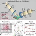
Small random library method combined with local searching in optical critical dimension measurements.​

Huawei Technologies Co. Ltd., Shenzhen 518000, China

Abstract​

The critical dimensions (CDs) of gratings significantly influence their optical performances and require high-resolution measurements. To avoid damaging the gratings, a model-based optical critical dimension (OCD) measurement method utilizing ellipsometry or scatterometry was applied by matching the simulated and experimental values. However, online CD measurements during grating fabrication require a bulky presimulated library containing the condition points with various CDs, making it time consuming and resource intensive to build with large dimension ranges to account for grating fabrication errors. In this study, we proposed a smaller random library with an unevenly distributed resolution, offering finer resolution when the grating to be measured is close to the reference grating. This approach, validated using a home-constructed spectroscopic ellipsometer, resulted in better results. Finally, a local search algorithm based on a random library was applied to further improve the measurement accuracy. This approach extraordinarily reduced the preparation time for OCD measurements and achieved better performance, significantly improving the efficiency of grating development and fabrication inspection.

1708381852463.png

Please, Log in or Register to view URLs content!
 

tokenanalyst

Brigadier
Registered Member

Peking University School of Integrated Circuits/Integrated Circuit Advanced Innovation Center has made important progress in the field of image storage system research.​


With the advent of the big data era and the rapid development of artificial intelligence, massive and rapidly generated multi-source data represented by images has brought severe challenges to the current storage system. Traditional image storage is based on the von Neumann computing architecture, using JPEG, JPEG2000, BPG and other encodings to compress images and store them in external memories such as mechanical hard drives and solid-state drives (flash memory). However, when dealing with current image storage needs, the above process still faces certain challenges: at the encoding level, the fixed pattern of time-frequency domain transformation and quantization matrix in traditional technology makes it difficult to deal with multi-source image data compression tasks. Obtain high-quality restored images and high compression efficiency at the same time; at the device level, external storage devices based on disks and flash memory have limited storage capacity of device units, which restricts the further improvement of storage density; at the architectural level, due to the external storage unit and processing The separation of the processor unit causes image data to need to be transmitted repeatedly during the compression and decompression process, resulting in a large amount of time and energy loss, which limits the improvement of storage efficiency.

1708386252816.png

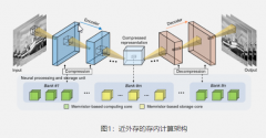
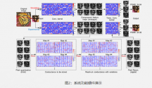
In response to the above key issues, the Peking University School of Integrated Circuits/Integrated Circuit Advanced Innovation Center research team proposed for the first time a near-external memory in-memory computing architecture for efficient compression-storage-decompression of multi-source image data (Figure 1 ). This architecture integrates external memory modules and in-memory computing modules into the same unit, and uses a memristor cross array to accelerate the image compression network, effectively reducing energy consumption and delays caused by data transfer. Based on this architecture, a storage system was built using memristor chips and convolutional autoencoder image compression networks, and a network mapping scheme and array operation mode suitable for image compression tasks were designed. At the same time, a step-by-step hardware perception training scheme and transposed convolution equivalent transformation are proposed to improve the reconstructed image quality and decoding efficiency of the storage system. Using the above design, the complete system functions including image compression/decompression and data storage/reading were demonstrated based on memristor chip hardware (Figure 2).

1708386270685.png

Furthermore, the storage system performance was evaluated based on the system construction and optimization plan. The results show that the delay and energy consumption in the image compression-storage-decompression process of the storage system based on the near-memory computing architecture are respectively reduced compared to the storage system based on the CPU/GPU under the von Neumann architecture. 20/5.6 times and 180/91 times. At the same time, the trained storage system has shown good compression and decompression effects on different types of image data sets, and the peak signal-to-noise ratio of the reconstructed images is greater than 33 dB. The proposed in-memory computing architecture of near-external memory in this study provides a new solution and technical path for energy-efficient and high-density storage of large amounts of multi-source data in the era of artificial intelligence.

Please, Log in or Register to view URLs content!
 

tphuang

Lieutenant General
Staff member
Super Moderator
VIP Professional
Registered Member
Chinese power chip expansion has led to significant decline in delivery time and likely price drop across the board


But of course, the Western govts will blame this as an evil overcapacity plot to destroy Western industries.

Maybe if those industries weren't so eager to limit capacity to maximize production, we wouldn't have this issue
 
Top