Look if Nvidia GPUs were snuggled then lithography stepper parts can also be snuggled. Each part is really small except for the lens. Lasers are the size of a show box for DUV. The worktable is quite heavy but made of multiple small parts. We might also see a lot of malicious compliance where they claim to comply with restrictions but don't enforce it themselves. For example, ASML ships the part to Singapore, South Korea or Taiwan or Japan. Parts are then purchased by third parties on second hand markets. Maybe parts can be cannibalised from used steppers. This is a nothingburger. At worst this is a shakedown attempt and ASML might make this go away with a few million dollar donation.Trump Team Seeks to Toughen Biden’s Chip Controls Over China.
Trump officials recently met with their Japanese and Dutch counterparts about restricting Tokyo Electron Ltd. and ASML Holding NV engineers from maintaining semiconductor gear in China, according to people familiar with the matter. The aim, which was also a priority for Biden, is to see key allies match China curbs the US has placed on American chip-gear companies, including Lam Research Corp., KLA Corp. and Applied Materials Inc.
The meetings come in addition to early discussions in Washington about sanctions on specific Chinese companies, other people said. Some Trump officials also aim to further restrict the type of Nvidia Corp. chips that can be exported to China without a license, Bloomberg News has previously reported. They’re also having early conversations about tightening existing curbs on the quantity of AI chips that can be exported globally without a license, said some of the people, who asked not to be identified because the deliberations are private.
One key measure is blocking Chinese memory chipmaker ChangXin Memory Technologies Inc. from buying American technology, a step that Biden officials seriously considered but ultimately did not pursue due to opposition from Japan.
Some officials on Trump’s team also want to intensify restrictions on Semiconductor Manufacturing International Corp., the main chipmaking partner to Chinese telecom giant Huawei Technologies Co. Biden effectively blocked shipments to some SMIC facilities but established a case-by-case review for others, which the officials worry could allow SMIC to purchase tools that are ultimately used at restricted plants. SMIC’s shares closed down 1.45% in Hong Kong.
You are using an out of date browser. It may not display this or other websites correctly.
You should upgrade or use an alternative browser.
You should upgrade or use an alternative browser.
Chinese semiconductor thread II
- Thread starter vincent
- Start date
This is a shakedown attempt for a donation. They just fired an export control official a few days ago. Musk will definitely have to beg Trump to reverse this because you know the reason.Given how down bad the relations between Europe and US are deteriorating, I wouldn't be surprised if they allow ASML to chip EUV machines to China. Also there is the issue that Trump is businessman not a politician, I think that the cries of the industry will have a bigger effect in Trump than lala land Biden. but let see what happens, US stupidity know no bounds so at the end is more domestic market share for Chinese companies.
Parts can be snuggled and chemicals even more easily. Trump just fired export control officials, so to be frank they themselves don't know what they plan to do and don't know how they plan to achieve it.basically requests ASML to stop the after service to equipments to China and japan to stop supplying photoresist.
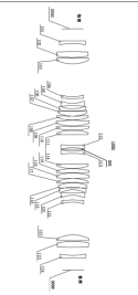
Chengdu Lianjiang Technology's new patent: Lithography objective lens exposure field of view exceeds 72mm×72mm, with broad prospects
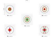
On the road of continuous advancement of optical technology, Chengdu Lianjiang Technology Co., Ltd. has once again attracted industry attention. According to information recently released by the State Intellectual Property Office, the patent named "Lithography Objective and Lithography Equipment" applied by the company in June 2024 was recently approved, and the authorization announcement number is CN222506637U. The core technological breakthrough of this patent makes the exposure field area of the lithography objective lens greater than or equal to 72mm×72mm and the resolution less than 780nm. This innovation will not only have a far-reaching impact in the fields of semiconductor manufacturing, microelectronics technology, etc., but also pave the way for a wider range of optical applications.
As a key component in the optical system, the photolithography objective lens is used to accurately transfer the designed pattern to the photoresist. In this patent of Chengdu Lianjiang Technology, the photolithography objective lens is composed of 20 lenses. The clever arrangement design allows the objective lens to expand the field of view while ensuring high resolution. This means that in the semiconductor industry, future photolithography equipment can perform high-precision pattern burning within a larger field of view, improve production efficiency and reduce costs.
When analyzing the lithography objective, we can see its uniqueness in lens design. The first and twentieth lenses adopt a planar design, while the remaining lenses combine positive and negative optical power structures. This composite design not only improves the imaging quality of the objective, but also effectively reduces chromatic aberration and optical distortion, greatly enhancing its reliability and adaptability in practical applications.
With the rapid development of semiconductor manufacturing technology, the accuracy and efficiency of lithography process have become increasingly key factors in competition. The emergence of this new patent just meets the industry's urgent need for high-performance lithography systems. Giants in the field of lithography, such as ASML and Tokyo Electron, are facing fierce challenges from emerging companies. Chengdu Lianjiang Technology is expected to occupy a place in the international market with its independently developed lithography objective lens.
In addition to the technical characteristics of lithography lenses, Chengdu Lianjiang Technology sees broader application prospects in the industry development trend. With the popularization of integrated circuits and optoelectronic components, the demand for high-resolution lithography equipment is growing significantly. Especially driven by emerging technologies such as 5G, artificial intelligence, and the Internet of Things, every link in the semiconductor industry chain is pursuing higher technical thresholds.
In this regard, Chengdu Lianjiang Technology plans to increase investment in research and development in its future development strategy to further improve the performance of lithography lenses. At the same time, the company is also actively cooperating with universities and research institutions to promote cutting-edge technology research and application in the field of optics. According to Tianyancha data, Chengdu Lianjiang Technology was established in 2019 with a registered capital of 10 million yuan. It has accumulated 103 patent information so far and actively participated in various bidding projects. Its current achievements in the field of optics have undoubtedly brought new vitality to the industry.
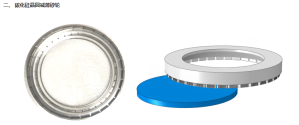
Changsha Sap New Materials independently developed the first domestic silicon carbide substrate 30000# fine grinding and thinning grinding wheel
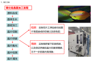
The core link in the silicon carbide production process is the processing of silicon carbide substrates, which is mainly divided into three processes: cutting, thinning and polishing of silicon carbide substrates. Thinning is mainly achieved through grinding and lapping, which are divided into rough grinding and fine grinding. The silicon carbide wafer thinning grinding wheel and grinding technology independently developed by Sap New Materials, from the wafer damage mechanism during the grinding process to the rough and fine grinding of the wafer, uses diamond grinding wheels to achieve wafer thinning processing with low damage and high cutting rate.
United Nova reporting huge gain in their revenue in 2024 vs 2023. Sales up 22.25%
auto and consumer electronics led the way.
They made progress sin microphone, IMU, pressure sensor, micro mirror, VCSEL, RF filters and power ICs.
It currently provides 70% of the chips in a car from analog to power chips to digital, sensors and modules.
for renewables, their 120 kW and 150 kW solar inverter is increasing market share. their 12tkW, 220kW and MW level power module for ESS customer has also started production
company has started mass production of 180nm process for tech for AI server power management chips, MOSFET for power management has also started
It is also going through customer product verification for 55nm BCD 20V integrated DrMOS.
Also mass production of MEMS sensors and power chip in robots and AI consumer electronics.
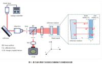
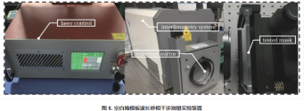
A wavelength phase-shifting interferometry method for synchronously measuring the surface morphology and thickness variation of a blank mask
Abstract
In the semiconductor lithography process, blank masks are primitive optical flats, and nanometer precision surface profiles play an important role in improving the performance of advanced chips. To measure the surface profile and thickness variation of a blank mask, a method is proposed based on parameter time-domain estimation for wavelength phase-shifting interferometry of a blank mask. First, to ensure the validity of the measurements, the coupling relationship between the front and rear surfaces of the blank mask and thickness variation is determined according to the optical path tracing method, and the self-assessment rule for the error in wavelength phase-shifting interferometry is analyzed. Next, to avoid the influence of spectral distortion and cavity length on accuracy, the parameter time-domain estimation method is used to determine the carrier parameters. Concurrently, the initial phase is demodulated based on the weighted least-squares principle to reduce the sensitivity of the algorithm to anisotropic noise. Finally, simulations are conducted to analyze the influence of different factors on the measurements. In addition, comparison experiments are carried out at different cavity lengths, with 10 -3 λ 0 as the magnitude of the blank mask interferometry error self-assessment index. The results show the effectiveness and stability of the proposed algorithm in measuring surface profiles and thickness variations of the blank mask, thereby providing a technical approach for advanced chip manufacturing.
In the semiconductor lithography process, blank masks are primitive optical flats, and nanometer precision surface profiles play an important role in improving the performance of advanced chips. To measure the surface profile and thickness variation of a blank mask, a method is proposed based on parameter time-domain estimation for wavelength phase-shifting interferometry of a blank mask. First, to ensure the validity of the measurements, the coupling relationship between the front and rear surfaces of the blank mask and thickness variation is determined according to the optical path tracing method, and the self-assessment rule for the error in wavelength phase-shifting interferometry is analyzed. Next, to avoid the influence of spectral distortion and cavity length on accuracy, the parameter time-domain estimation method is used to determine the carrier parameters. Concurrently, the initial phase is demodulated based on the weighted least-squares principle to reduce the sensitivity of the algorithm to anisotropic noise. Finally, simulations are conducted to analyze the influence of different factors on the measurements. In addition, comparison experiments are carried out at different cavity lengths, with 10 -3 λ 0 as the magnitude of the blank mask interferometry error self-assessment index. The results show the effectiveness and stability of the proposed algorithm in measuring surface profiles and thickness variations of the blank mask, thereby providing a technical approach for advanced chip manufacturing.
how far we are from chinese euv?
Go back and read through this thread. It has been discussed many times.
-IMO way closer than most people give them credit.how far we are from chinese euv?
-Given the surge of mask and inspection patents looks like they are already patterning wafers.
-So looks like they already have hardware being tested.
-They are going High. There is not other way around, why having that level of optics just for toying around, in a lithography machine the optics determine everything in the design, from the light source to the body frame.
