BYD ramping up hiring across its semi fabs to deal with the demand from rolling out ADAS across its lineup
You are using an out of date browser. It may not display this or other websites correctly.
You should upgrade or use an alternative browser.
You should upgrade or use an alternative browser.
Chinese semiconductor thread II
- Thread starter vincent
- Start date
InnoLaser officially launched the laser high-speed punching and cutting equipment (HTLC series) for FPC forming mass production cutting. This equipment is different from the previous laser proofing and cutting machine. It can completely replace the traditional mold punching and cutting process. While the efficiency is comparable to that of a punching machine, it improves product precision - automatically compensates for product expansion and contraction, saves mold costs - flexible manufacturing process, improves material utilization - zero spacing layout, shortens production cycle - single laser forming replaces multiple mold punching and cutting, and achieves safe production, bringing a new laser cutting solution to the FPC industry. It is suitable for consumer electronics, industrial control, automotive, new energy, modules, light strips and other products, especially products after patching


The latest progress of domestic advanced processes (clear card, institutional research report)
1. The advanced process N+3 process is close to the mass production window. Don't call it equivalent to 5nm, 5.5nm or 6nm, it's all the same thing, from the N+3 process platform.
2. 3D DRAM is close to domestic production and mass production. In fact, from the perspective of storage and computing, this is also a big deal.
3. HBM2e is basically running through, which many sellers have mentioned before. The key is when will the subsequent HBM3 run through.
4. Many design factories have begun to adjust their designs to fit the 7nm process or 7nm sealing process to adapt to the subsequent domestic advanced process expansion.
5. The expansion of advanced process production is certain this year.
6. Overseas computing power procurement of large factories has become tense, and it is already difficult to get H20. Capital expenditures are beginning to expand rapidly again.
Therefore, based on 1, 2, 3, and 4, we can draw the first inference: We have completed the breakthrough of the entire chain to within 7nm, but there are still problems with testing, wafer yield, and packaging running-in, etc., which are all process problems.
Combining push wheel 1 and 5, we can draw the second inference: After the expansion of production and the process running-in, we can basically achieve the expansion of 7nm and 7nm-based sealing supply.
Inferences 1 and 2 and point 6 complete the logical closed loop. While demand is expanding, supply is expanding, and product capabilities are improving.
so within the year, we can see: 7nm maturity + expansion, N+3 running-in/breakthrough, process plus one generation, HBM plus one generation, Ascend plus one generation, Kirin plus one generation, production capacity continues to be tight, storage and computing continue to expand, and external unstable factors are avoided as much as possible. In addition, the computing power card is not only Huawei Ascend, HWJ HG SY and other points blossom
The lithography machine is steadily advancing as planned, and the replacement of equipment/materials is more important. EDA is not worried at all. It is mature and cheap, and Korean manufacturers have begun to purchase it (already used)
Tsinghua University School of Integrated Circuits team collaborates to develop co-evolutionary brain-computer interface based on memristor brain-like computing chip
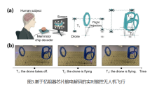
the School of Integrated Circuits of Tsinghua University and the Haihe Brain-Computer Laboratory of Tianjin University have collaborated to propose a new brain-computer interface solution based on a memristor-like brain computing chip. The team developed a 128Kb memristor chip as an adaptive EEG decoder, built a complete brain-computer interface system (including EEG acquisition, decoding and actuator), proposed a single-step decoding strategy and an interactive update framework, and achieved long-term stable, efficient and high-precision EEG decoding and brain-computer co-evolution.
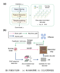
The single-step decoding strategy adopted by the memristor chip integrates the three-step decoding process of the steady-state visual evoked potential (SSVEP) EEG intention signal (signal filtering preprocessing, task-related component feature extraction, template matching classification) into a single step, reducing the computational complexity by 6.5 times and reducing the impact of the non-ideal characteristics of the memristor on the computational accuracy. In the four-degree-of-freedom real-time brain-controlled drone flight mission, the decoder achieved a decoding accuracy rate (85.17%) comparable to that of software calculation. Computational evaluation shows that the energy consumption of memristor chip decoding is three orders of magnitude lower than that of traditional CPUs, and the normalized processing speed is increased by two orders of magnitude.
Beijing Institute of Quantum, in cooperation with Tsinghua University and North China University of Technology, has successfully developed a one-way quantum direct communication system, setting a world record for long-distance stable transmission of 2.38kps @ 104.8km @168 hours.
The relevant results were published in the internationally renowned journal Science Advances under the title "Simultaneous transmission of information and key exchange using the same photonic quantum states" , marking the successful transition of quantum direct communication from theoretical conception to practical application .
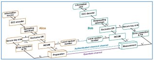
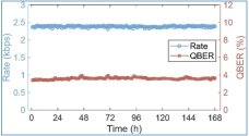
The relevant results were published in the internationally renowned journal Science Advances under the title "Simultaneous transmission of information and key exchange using the same photonic quantum states" , marking the successful transition of quantum direct communication from theoretical conception to practical application .


What are the models and prices of lithography machines sold by ASML?
According to statistics, from 2012 to 2023, ASML shipped 2,235 DUV lithography machines. In 2023, ASML sold 449 lithography machines, of which 53 were EUV lithography machines and 396 were DUV lithography machines. A large part of the shipments of DUV lithography machines in 2023 came from the Chinese market.
Because at the end of 2023, the latest export control regulations issued by the Netherlands and the United States have come into effect. At that time, ASML's Chief Financial Officer Roger Dassen said: "In 2024, we will not obtain an export license for shipping NXT:2000i and above immersion equipment to China. In addition, some Chinese advanced chip manufacturing wafer factories will not be able to obtain a license to ship NXT:1970i and NXT:1980i immersion equipment."
The purchase amount of lithography machines in mainland China has remained at around 2 billion euros, but it soared by 6.1 billion euros in 2023.
In other words, we will do our best to buy as many lithography machines as possible before the ban comes down.
From 2012 to 2023, AMSL shipped a total of 233 EUV lithography machines. The unit price of the dual-stage EUV lithography machine currently sold by ASML is about US$120 million to US$150 million. And its new generation of high-NA EUV lithography machines costs as much as 300 million to 350 million euros (approximately RMB 2.195 billion to 2.561 billion).
In 1991, ASML launched the PAS 5500 system. To this day, this model is still ASML's most youthful lithography equipment and one of the most widely used product lines. Its resolution ranges from 400nm to 90nm, and the registration accuracy ranges from 100nm to 12nm. As of now, ASML has many lithography machine models. The following table data are all from the data published on ASML's official website
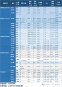
Below are the prices of some models of lithography machines, for reference only.
1. **TWINSCAN EXE:5000** - **Price**: about 350 million euros (about 2.63 billion yuan), belonging to the first generation of High NA equipment, mainly used for technology development. - **Features**: Supports advanced processes of 2nm and below, aperture lens accuracy of 0.55, and wafer throughput of more than 185 pieces per hour. 2. **TWINSCAN EXE:5200** - **Price**: Not clearly disclosed, but expected to be higher than EXE:5000, possibly more than 400 million euros. - **Features**: Optimized version of High NA lithography machine, more suitable for large-scale production, further improved throughput and stability, supporting post-2nm process.
2. Low NA EUV lithography machine (low numerical aperture extreme ultraviolet lithography machine)** 1. **NXE:3800E** - **Price**: about 250 billion won (about 1.317 billion yuan), belonging to traditional Low NA equipment. - **Features**: The aperture lens precision is 0.33, and the wafer throughput of the latest model has been increased to 220 wafers per hour, supporting 7nm and below processes.
III. Immersion DUV Lithography Machine (Deep Ultraviolet Lithography Machine)** 1. **1980Di** - **Price**: Not disclosed, but it is a mid-range device with a significantly lower price than EUV models. - **Features**: It can support 7nm process through multiple exposure technology and is used by Chinese companies to expand production of mature processes. 2. **2000i** - **Price**: Not specified, but higher than 1980Di, it is a more advanced DUV model. - **Features**: The Netherlands recently approved exports to China, supporting more efficient multiple exposure processes, close to 7nm performance.
IV. Future Planning Models 1. **Hyper NA EUV Lithography Machine (0.75 NA)** - **Expected Price**: It will be launched in 2030, and the unit price may exceed 1 trillion won (about 5.267 billion yuan), which is twice that of the High NA model. - **Positioning**: Aiming at 1nm and below processes, but TSMC, Samsung and other manufacturers are currently waiting to see whether to introduce it.
V. Summary
- **Price trend**: The cost of lithography equipment continues to rise, and the price of a single High NA EUV has exceeded 350 million euros. The equipment cost has become an important consideration for foundries to choose the process route.
- **Customer distribution**: Intel is the first customer of High NA EUV, while TSMC and Samsung have not yet disclosed their procurement plans; the demand in the Chinese market is concentrated on DUV equipment, accounting for 20%~40% of ASML's revenue.
CXMT coming with own solutions for lithography equipment maintenance?

Background Art
There are many water pipes under the workbench of the lithography equipment, which provide cooling for the normal operation of the workbench and keep the temperature of the machine engine and the workbench constant. As the working time of the lithography equipment increases, water leakage is inevitable in the pipes. Once the leaking water drips onto the grating ruler below, the positioning accuracy of the machine will deviate, which will cause the machine to shut down.
Therefore, there is an urgent need for a solution that can monitor the leakage of cooling water pipes of lithography equipment.
The above information disclosed in the background technology section is only used to enhance the understanding of the background technology of the technology described in this article. Therefore, the background technology may contain certain information that does not form the prior art known in this country for those skilled in the art.
Summary of the invention
The main purpose of the present application is to provide a lithography device to solve the problem in the prior art of lacking a solution for monitoring water leakage in the cooling water pipe of the lithography device.
According to one aspect of an embodiment of the present invention, there is provided a lithography device, comprising: a shell having a accommodating cavity; a workbench located in the accommodating cavity, the workbench comprising a cooling device and an optical structure, the cooling device being arranged around the periphery of the optical structure, the optical structure being used to receive a light beam; a grating scale located on the inner wall of the shell; a color-changing structure located on the inner wall of the shell between the grating scale and the cooling device, the color of the color-changing structure changing when in contact with liquid; and a detection device, used to obtain color information of the color-changing structure, and determine whether liquid leakage occurs in the cooling device based on the color information of the color-changing structure.

Korean Institute Report: Most Semiconductor Technologies Have Been Overtaken by China
According to Yonhap News Agency, a survey report released by the Korea Institute of Science and Technology Evaluation and Planning (KISTEP) on the 23rd pointed out that most of South Korea's semiconductor technologies have been overtaken by China
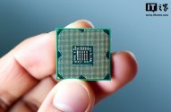
According to Yonhap News Agency, a survey report released by the Korea Institute of Science and Technology Evaluation and Planning (KISTEP) on the 23rd pointed out that most of South Korea's semiconductor technologies have been overtaken by China

Dalian University of Technology team has made the latest breakthrough in flexible electro-hydraulic power chips
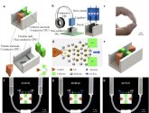
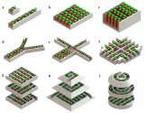
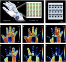
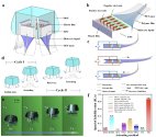
Professor Xu Changyi of the School of Control Science and Engineering of Dalian University of Technology published a research result in Nature Communications with Professor Zhang Chao and Professor Zhu Yi of the School of Mechanical Engineering of Zhejiang University as the co-corresponding author. The Flexible electro-hydraulic power chips "chip" the multi-channel fluid power source through modular logic design ideas, thus realizing multi-channel drive and complex control of small robot systems and high power density output. This technology may provide new lightweight and portable solutions for small robots, wearable devices, etc


Professor Xu Changyi of the School of Control Science and Engineering of Dalian University of Technology published a research result in Nature Communications with Professor Zhang Chao and Professor Zhu Yi of the School of Mechanical Engineering of Zhejiang University as the co-corresponding author. The Flexible electro-hydraulic power chips "chip" the multi-channel fluid power source through modular logic design ideas, thus realizing multi-channel drive and complex control of small robot systems and high power density output. This technology may provide new lightweight and portable solutions for small robots, wearable devices, etc
