Chinese semiconductor thread II

tphuang

Lieutenant General
Staff member
Super Moderator
VIP Professional
Registered Member
You just answered it yourself. HBM is DRAM dies stacking,thus HBM speed is proportional to DRAM speed,newer faster HBM requires newer faster DRAM.
there is no where that says you need a certain process. For example, DDR5 implemented by CXMT is around 16nm, but it can be implemented much smaller features, all the down to D1b by other players.

Now, if we take a look at this TechInsights road map that you posted earlier for DRAM technology roadmap, it showed D1b for HBM3E and D1z for HBM3.

But for Samsung, it had D1a, 14nm, DDR5/LPDDR5X/HBM3/HBM3E

So there isn't any necessity for HBM3E to be D1b.

That's in the picture you posted.
 

tphuang

Lieutenant General
Staff member
Super Moderator
VIP Professional
Registered Member
SMEC/United Nova has seen itself swing into profitable margin for the first time in 2024

Please, Log in or Register to view URLs content!

Revenue was 6.509B RMB and up 22.26% YoY

It achieved positive annual gross profit margin for the first time, reaching 1.1%

It's net profit loss was reduced by 50.5% to 969m RMB.

Has signed LTAs with NIO, Li Auto & GAC for SiC products and more

It achieved > 1B RMB in SiC revenue and now using 8 inch wafers

It also developed high voltage late power BCD
 

tokenanalyst

Brigadier
Registered Member
Possible metrology tool for 3D-NAND and EUV mirrors. It could surpass traditional film thickness metrology methods in precision.​

Model-based thickness estimation of multilayer films in picosecond ultrasonics metrology with aliased echoes.​

Abstract​

Picosecond ultrasonics (PU) combines the advantages of optical and acoustic measurements, and also provides nanoscale longitudinal resolution, making it the workhorse technique for in-line thickness measurement of opaque submicron films. In PU measurements of multilayer films, echo aliasing often occurs and leads to inaccurate thickness estimation based on straightforward time-domain analysis. This work proposes a model-based thickness estimation method for cases where some echoes are aliased, forming discrete echo-signal regions. The model used is lightweight and does not rely on reference signals obtained from standard specimens. Specifically, a theoretical model is developed to reflect the spectrum relationship between different echo-signal regions in one measurement curve, and is then used to fit the measured spectrum relationship to inversely extract thicknesses. Simulations are conducted and yield ways to reduce noise impact. Eventually, the proposed method is validated through PU measurements of submicron W/Al bilayer films, with estimation errors within 2.3%.​


Please, Log in or Register to view URLs content!

Please, Log in or Register to view URLs content!
 

tokenanalyst

Brigadier
Registered Member

Innoscience launches full range of data center products, further upgrading energy saving and efficiency improvement!​


Data centers are the core infrastructure of cloud computing, responsible for centralized storage, computing and exchange of data. With the rapid development of technologies such as the Internet of Things and artificial intelligence, data centers are further evolving into smart data centers. Data and computing volumes are growing exponentially, and energy consumption is also increasing dramatically. Improving system efficiency and reducing energy consumption are key.

Wide bandgap semiconductor (third generation semiconductor) gallium nitride (GaN) can greatly improve the power supply efficiency of data centers and significantly reduce energy consumption due to its excellent high frequency, high efficiency and low loss characteristics. As the global leader in third generation semiconductor gallium nitride, Innoscience has always been committed to the research and development and innovation of gallium nitride products. For the data center field, it has developed a series of discrete and integrated gallium nitride products that can maximize efficiency and reduce energy waste.

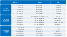
For the front-end input side of the data center - server power supply PSU (PFC/LLC) 1kW-4kW AC/DC link, Innoscience has launched 15 power devices, driver chips and packaged chips to create a high-efficiency, low-power PSU with titanium energy efficiency to achieve server stability and reliability.

1737058678613.png

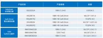
In the motherboard power supply applications of data centers, Innoscience has a total of 8 discrete and integrated chips to meet the high efficiency and high power density requirements of the 54-12V power supply link.

1737058717297.png

Please, Log in or Register to view URLs content!
 

tokenanalyst

Brigadier
Registered Member
Possible metrology tool for 3D-NAND and EUV mirrors. It could surpass traditional film thickness metrology methods in precision.​

Model-based thickness estimation of multilayer films in picosecond ultrasonics metrology with aliased echoes.​

Abstract​

Picosecond ultrasonics (PU) combines the advantages of optical and acoustic measurements, and also provides nanoscale longitudinal resolution, making it the workhorse technique for in-line thickness measurement of opaque submicron films. In PU measurements of multilayer films, echo aliasing often occurs and leads to inaccurate thickness estimation based on straightforward time-domain analysis. This work proposes a model-based thickness estimation method for cases where some echoes are aliased, forming discrete echo-signal regions. The model used is lightweight and does not rely on reference signals obtained from standard specimens. Specifically, a theoretical model is developed to reflect the spectrum relationship between different echo-signal regions in one measurement curve, and is then used to fit the measured spectrum relationship to inversely extract thicknesses. Simulations are conducted and yield ways to reduce noise impact. Eventually, the proposed method is validated through PU measurements of submicron W/Al bilayer films, with estimation errors within 2.3%.​


Please, Log in or Register to view URLs content!

Please, Log in or Register to view URLs content!


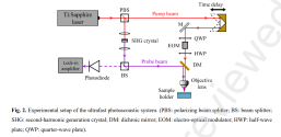
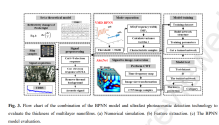
Basically the setup and then use a neural network for the classification.
1737059174169.png1737059252015.png

Please, Log in or Register to view URLs content!
 

tokenanalyst

Brigadier
Registered Member

Tuojing Technology plans to acquire a stake in Shenzhen Guanhua, a leading domestic company in the field of vacuum instrumentation, to enhance the stability of the upstream supply chain​


Tuojing Technology issued an announcement that its wholly-owned subsidiary Yanquan Technology Co., Ltd. intends to subscribe to the additional registered capital of Guanhua of RMB 147,610 with RMB 15 million, accounting for 2.479% of the equity of Guanhua after this transaction, and at the same time, it intends to transfer the registered capital of Guanhua held by the original shareholders of RMB 451,030 with RMB 3,750,000, accounting for 0.758% of the equity of Shenzhen Guanhua after this transaction. After the completion of the above transaction, Yanquan Technology will account for 3.237% of the equity of Guanhua after this transaction.

It is reported that Guanhua has deployed a variety of core components around the vacuum chamber in semiconductor front-end process equipment, with differential pressure gas mass flowmeter as the core product, and other products including vacuum gauges, evaporators, etc. Guanhua takes semiconductor front-end equipment and wafer factories as its main downstream customers, and in the future it can expand to photovoltaic equipment, panel equipment, and other industrial fields. It is an important manufacturer of 12-inch differential pressure mass flowmeters in the domestic semiconductor field.

Guanhua has made breakthroughs in the field of domestic vacuum instrumentation, and is in a leading position in the domestic industry. It has been recognized by domestic semiconductor equipment industry customers and has obtained batch shipments. The verification work in domestic wafer fabs is also progressing steadily, with great growth potential and investment value. This time, Yanquan Technology and the company's related party Fuchuang Precision jointly invested in Shenzhen Guanhua, which will help the company promote the coordinated development of the industry, enhance the stability of the upstream supply chain, and assist in the implementation of the company's strategic planning.​
 

mst

Junior Member
Registered Member

US bans sales of 14nm and 16nm chips with over 30 billion transistors to China​

The U.S. government plans to unveil stricter regulations to block shipments of advanced processors made by TSMC, GlobalFoundries, Intel, and Samsung Foundry to China. By 'advanced,' the new rules mean processors made on 14nm or 16nm process technologies or more advanced that contain 30 billion transistors or more, according to Bloomberg. But there will be exceptions.

The new rules target chips with 30 billion transistors made on 14nm or 16nm nodes or smaller, as such products are presumed to be restricted for shipment to entities in China and other restricted nations unless their developers get an export license from the U.S. Department of Commerce. Chip designers from the U.S., Taiwan, or an allied nation can apply for a license if they sell to 'authorized customers.' Also, processors with fewer than 30 billion transistors and packaged by a trusted company would not be classified as advanced and, therefore, would not fall under the new restrictions, according to Bloomberg's sources.

But while the new export rules have little to do with the vast majority of chips for client devices, they force AMD, Intel, and Nvidia to apply for an export license when selling mainstream GPUs to a Chinese entity, even if that GPU was previously deemed unrestricted because its AI performance was not considered powerful enough for severe applications. This could impact Nvidia significantly.

Please, Log in or Register to view URLs content!
 

Wahid145

Junior Member
Registered Member

US bans sales of 14nm and 16nm chips with over 30 billion transistors to China​

The U.S. government plans to unveil stricter regulations to block shipments of advanced processors made by TSMC, GlobalFoundries, Intel, and Samsung Foundry to China. By 'advanced,' the new rules mean processors made on 14nm or 16nm process technologies or more advanced that contain 30 billion transistors or more, according to Bloomberg. But there will be exceptions.

The new rules target chips with 30 billion transistors made on 14nm or 16nm nodes or smaller, as such products are presumed to be restricted for shipment to entities in China and other restricted nations unless their developers get an export license from the U.S. Department of Commerce. Chip designers from the U.S., Taiwan, or an allied nation can apply for a license if they sell to 'authorized customers.' Also, processors with fewer than 30 billion transistors and packaged by a trusted company would not be classified as advanced and, therefore, would not fall under the new restrictions, according to Bloomberg's sources.

But while the new export rules have little to do with the vast majority of chips for client devices, they force AMD, Intel, and Nvidia to apply for an export license when selling mainstream GPUs to a Chinese entity, even if that GPU was previously deemed unrestricted because its AI performance was not considered powerful enough for severe applications. This could impact Nvidia significantly.
Please, Log in or Register to view URLs content!
They are becoming more and more paranoid by the day and a total laughing stock to us. I remember 3-4 years ago, whenever america put restrictions on Huawei and SMIC or YMTC, I used to get so worried about the Chinese Semiconductor Industry (and quite mad at the author of article preceding the sanction on a specific company). But for last year or so whenever I see stupid sanctions like this, a smile appears in my face because all these new restrictions doing is fueling Chinese self sufficiency further and further (except for sanctions related to ASML 2050i perhaps, China still needs those as of now).

Finally this 14nm ban just another blessing in disguise for SMIC and I'm sure gonna incentivize HuaHong to get their act together to develop that 14nm FinFet they have been talking about for ages
 

Phead128

Captain
Staff member
Moderator - World Affairs

Please, Log in or Register to view URLs content!

The implosion of Apple's marketshare in China and implosion of Intel is inversely correlated to rate of US sanctions applied to China. The reality is that most consumers cannot tell the difference between 3nm and 7nm on mobile phone unless you doing data decryption on your phone or perhaps hardcore mobile gaming. Even then, it's not a deal breaker for running email, web browsing, or video apps.
 
Top