Chinese semiconductor thread II

sunnymaxi

Major
Registered Member
Do we know whether the Mate 70 RF is the same as on the Mate 60 or has it been upgraded significantly?
that was the first high end model from Huawei after cut off from TSMC, google service and US technologies. even if RF performance was not that good. this was just the beginning.

Mate60 was the first step of ladder and had many older technologies include foreign components from Korea/Japan.

after that Huawei released Pura70 , Nova series and Mate70. these devices definitely have superior RF. we all know that how capable Mate70 is.. this year Pura80/Mate80 series coming. means Huawei keep innovating and upgrading its tech base.

tonyget is a clown.. if you follow his pattern, he always do this. appeared from nowhere and posted some of old information and slander China to have inferior technology.
 

leibowitz

Junior Member
that was the first high end model from Huawei after cut off from TSMC, google service and US technologies. even if RF performance was not that good. this was just the beginning.

Mate60 was the first step of ladder and had many older technologies include foreign components from Korea/Japan.

after that Huawei released Pura70 , Nova series and Mate70. these devices definitely have superior RF. we all know that how capable Mate70 is.. this year Pura80/Mate80 series coming. means Huawei keep innovating and upgrading its tech base.

tonyget is a clown.. if you follow his pattern, he always do this. appeared from nowhere and posted some of old information and slander China to have inferior technology.
Tonyget is in the industry and has a high bar for credibility. Good to have a devil's advocate here...
 

tphuang

Lieutenant General
Staff member
Super Moderator
VIP Professional
Registered Member
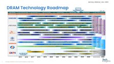
fyi, you can find these clips also just on techInsights website once you sign up to them.

It's not bad information on memory chip industry as a whole.

I think someone posted a synopsis after the progress earlier. I'm not sure if what was state for CXMT is necessarily true, but it had this

  • CMT: We are currently developing the G5 generation [DDR4/5, LPDDR5/5X, HBM3] and expect to enter 10mm or below as early as the end of 2026 or early 2027.
That was kind of cool.
 

tonyget

Senior Member
Registered Member
fyi, you can find these clips also just on techInsights website once you sign up to them.

It's not bad information on memory chip industry as a whole.

I think someone posted a synopsis after the progress earlier. I'm not sure if what was state for CXMT is necessarily true, but it had this


That was kind of cool.

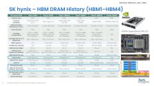
According to the snapshot,HBM3E requires DRAM tech node H-D1b,I'm not sure where is CXMT now
 

diadact

New Member
Registered Member
According to the snapshot,HBM3E requires DRAM tech node H-D1b,I'm not sure where is CXMT now
They will probably get to 12nm=D1b within the next 18 months and D1z with HKMG is enough for HBM3
I expect Ascend 920/910D(late 2025 or Q1 2026) to ship with CXMT's HBM3
They are already mass-producing HBM2
The 2022 export controls delayed their plans by 2 years
 

tonyget

Senior Member
Registered Member
They will probably get to 12nm=D1b within the next 18 months and D1z with HKMG is enough for HBM3

Samsung and Hynix get to 12nm=D1b with EUV,I don't know how CXMT could do it with DUV

They are already mass-producing HBM2
I expect Ascend 920/910D(late 2025 or Q1 2026) to ship with CXMT's HBM3

Where is evidence that CXMT already mass-producing HBM2?
 

tphuang

Lieutenant General
Staff member
Super Moderator
VIP Professional
Registered Member
According to the snapshot,HBM3E requires DRAM tech node H-D1b,I'm not sure where is CXMT now
I don't know if that's a fast rule. HBM is just stacking a bunch of DRAM dies together. Why does it need to be D1b to work?

And I don't know why you are bringing HBM3E here, when the more realistic option is they get to HBM3 first.
 

tonyget

Senior Member
Registered Member
I don't know if that's a fast rule. HBM is just stacking a bunch of DRAM dies together. Why does it need to be D1b to work?

You just answered it yourself. HBM is DRAM dies stacking,thus HBM speed is proportional to DRAM speed,newer faster HBM requires newer faster DRAM.
 

tokenanalyst

Brigadier
Registered Member

Growth and characterization of SiGe/Si superlattice for vertically stacked DRAM.​

Abstract​

In this study, SiGe/Si superlattices films (SLs) with different tiers were epitaxially grown by reduced pressure chemical vapor deposition (RPCVD) on 300 mm Si (001) substrate. Crystal quality of SiGe/Si SLs films (relaxation, surface roughness, interface characteristics and dislocation density) were quantitative evaluated by various characterization methods. A systematic investigation was conducted on the transition process of the SiGe/Si SLs films from full strain to relaxation state with increasing stacking layers. And, the variation trend of dislocation density and surface roughness with increasing stacking layers is studied. Additionally, we examined the changes in crystal quality and dislocation density of these SLs films after thermal annealing (20 min, @700 °C), and all the films exhibit higher strain relaxation by generating more misfit dislocations propagating in-plane. This study provides guidance and reference for the regulation of process parameters and the design of superlattice structure in vertically stacked DRAM.

Please, Log in or Register to view URLs content!
 
Top