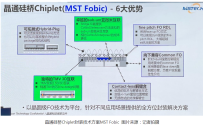
MST Fobic, a chiplet packaging technology solution of Jingtong Silicon Bridge.

The TMV technology enables the Crystalbridge Chiplet to achieve 2.5D/3D interconnection, which can improve the connection density and performance between chips. At the same time, it avoids the TSV re-design problem and reduces design complexity and cost.
Jingtong Silicon Bridge Chiplet can flexibly implement BGA/Bump packaging, and can also be integrated with the substrate to form a hybrid package. This optimized structure can meet the needs of different application scenarios. By adopting the Face up FO method, 2um level Fine Pitch RDL can be achieved. This high-density redistribution layer design surpasses traditional solutions such as eWLB and helps to achieve a more compact packaging design.
In addition, the Chiplet technology of Crystalbridge provides an excellent bonding and debonding method, which can achieve a position accuracy of ±1 micron, which is crucial to improving packaging yield and reliability.
With the continuous development of the semiconductor industry, silicon bridge chiplets are expected to become the mainstream trend of advanced packaging. This technology, with its unique advantages such as high wiring accuracy, high package pin density, and small package size, meets the demand for ultra-high density packaging in high-performance computing, networking and other fields.
At present, Silicon Bridge Chiplet technology has been widely used in high-performance computing fields such as AI servers, AI mobile phones, and AI PCs, becoming one of the key technologies to promote the development of these fields. Data shows that the market share of Silicon Bridge packaging solutions will reach 24% in 2024 and is expected to reach 55% in 2025. The technology shows strong market growth potential.


