Chinese semiconductor thread II

tokenanalyst

Brigadier
Registered Member

Longsys' self-developed SLC NAND Flash has shipped over 100 million pieces!​

Longsys, a major domestic memory chip manufacturer, announced that the company has fully utilized its chip design capabilities and continued to actively invest in memory chip design business. As of now, the cumulative shipments of its self-developed SLC NAND Flash have exceeded 100 million!

In the first half of 2024, the company launched a new generation of 2Gbit SPI NAND Flash chip products based on 2xnm, with an interface speed of up to 166MHz and support for DTR (double transmission) function to achieve higher data transmission rates. Based on SLC NAND Flash products, the company also uses multi-chip packaging technology to integrate SLC NAND storage particles with LPDDR storage particles, and expands NAND based MCP products with various specifications. In addition to the existing SLC NAND and LPDDR2 integrated package MCP products, in the first half of 2024, SLC NAND and LPDDR4x integrated package MCP products were also launched, which are mainly used in 5G communication modules and have entered small-scale production.

The company's self-developed memory chip products implement quality management throughout the production process, achieve particle-level traceability, and have a DPPM (defective products per million defect opportunities) of less than 100, with outstanding performance and stability. Shipments are growing rapidly in consumer, industrial and automotive application scenarios, with cumulative shipments exceeding 100 million units to date.​

1731685906286.png
Please, Log in or Register to view URLs content!
 

tokenanalyst

Brigadier
Registered Member

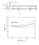
Beam matching method and device for laser amplification system​

Changchun Institute of Optics Fine Mechanics and Physics of CAS

Abstract​

The invention relates to the technical field of extreme ultraviolet lithography, in particular to a method and a device for matching a laser amplifying system beam, which are characterized in that a variable curvature reflector is inserted between a seed laser and a laser amplifier based on the existing laser amplifying system, a space optical filter is inserted behind the laser amplifier, the space optical filter can effectively block transmission of diffraction stray light generated by interaction of seed laser and the inner wall of the laser amplifier, a laser power meter is utilized to measure net laser power after the stray light is filtered by the space optical filter, and curvature of the variable curvature reflector is adjusted according to net laser power feedback, so that the beam transmission parameters of the seed laser beam in the laser amplifier are dynamically regulated and controlled, and the problem of mismatching between the seed laser parameters and the gain space of the laser amplifier caused by factors such as non-uniformity of light refractive index of a gas subsonic flow field and nonlinear amplification of the optical power of the laser amplifier at present is solved.​

1731688120363.png
 

tokenanalyst

Brigadier
Registered Member

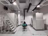
Gallium Semiconductor · New Plant | VB method crystal growth equipment is fully put into production!​


The official opening of the second phase of the factory of Hangzhou Gallium Semiconductor Co., Ltd. (hereinafter referred to as "Gallium Semiconductor") marked the further deepening of the company's strategic layout in the field of gallium oxide and the qualitative leap in production capacity. The new factory has introduced advanced industrial equipment in key links such as crystal growth, wafer processing and epitaxial growth , and is expected to significantly increase production capacity to meet the growing demand for gallium oxide wafer substrates and epitaxial wafers in the global market.

1731688978188.png


In the second phase of the factory, the vertical Bridgman method (VB method) dedicated gallium oxide crystal growth furnace independently developed and sold by Gallium Ren Semiconductor has been fully put into production and the process is continuously optimized on the existing basis. Bridgman method is a globally recognized key technology for the industrialization of gallium oxide. As the only domestic suppliers that can provide such equipment, we are committed to promoting the rapid development of the gallium oxide industry and look forward to working with more customers to solve industry problems."

With the introduction of the new production line, Gallium Semiconductor will further enhance the production capacity of gallium oxide materials and equipment to meet the growing market demand for high-performance semiconductor materials and special equipment. The introduction of the new production line will enable the company to achieve a new leap in product quality, production efficiency and cost control, and provide customers with better products and services.

Please, Log in or Register to view URLs content!
 

tokenanalyst

Brigadier
Registered Member

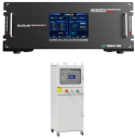
Guolin Semiconductor showcasing semiconductor grade ozone generators used in the cleaning of lithography machines.​


1731697677672.png
Guolin Technology-----The core multiple exposure cleaning equipment of the lithography machine!

(1) The company's semiconductor ozone equipment can be used for semiconductor cleaning, helping the localization of the industrial chain. Ozone technology is widely used in cleaning of various semiconductor process links. In the photolithography process, the VOS process (mixture of high-concentration ozone gas and vaporized water) can replace the traditional SPM (sulfur peroxide mixture) cleaning process.

(2) The company has made breakthroughs in the core technology of semiconductor ozone equipment, and its performance is comparable to that of the overseas leader MKS. The current product samples have been sent to downstream leading customers such as North Huachuang, Tuojing Technology, and BOE for verification. It is expected that the production line verification will be completed by the end of May 2024, and mass production can be put into operation immediately after the verification is completed.

(3) The potential space for front-end cleaning is conservatively 18e, and the potential space for thin film deposition is 20e. If the comprehensive localization rate reaches 10%, Guolin Technology's order profit for semiconductor equipment will start at 85 million yuan, and a market value of about 20e at 25pe. It will be difficult to have competitors within 2 years, and it will not be difficult to achieve a 30% market share in its main business of ozone generators in the medium term.


Please, Log in or Register to view URLs content!
 

GulfLander

Senior Member
Registered Member
"Chinese researchers have developed a new type of real-time imaging sensor that can detect whether food has spoiled or heavy metals in water exceeded safe standards with just a glance.

According to a study paper published in the journal Nature on Thursday, a research team from Beijing Institute of Technology (BIT) has developed the world's first hundred-channel, million-pixel hyperspectral real-time imaging device, showing broad application prospects in remote sensing, life and health, smart agriculture and industrial automation."

Please, Log in or Register to view URLs content!
 

european_guy

Junior Member
Registered Member

Beijing plans 12-inch wafer fab, pouring US$4.6 billion into state-backed chip project​


Please, Log in or Register to view URLs content!

Beijing Yandong Microelectronics will take a controlling position with a 25 per cent stake, while other investors include display maker BOE Technology

This new 12" fab is for mature nodes, possibly 65nm according to
Please, Log in or Register to view URLs content!
.

YDMC is famous to be the test site of the first SMEE prototype a couple of years ago, a DUV KrF machine IIRC.

And
Please, Log in or Register to view URLs content!
that equipment will be mostly domestically sourced:

BOE's investment is for Yandong Microelectronics to build a 12-inch wafer fab using domestic IC manufacturing equipment and conducting production process verification of the equipment.

IMHO, considering that the project starts now and it is a 65nm node, this fab will be fully domestic, litho machines included.
 

tokenanalyst

Brigadier
Registered Member

China's first printed OLED display goes into mass production, TCL Huaxing launches new technology brand APEX​


On November 16, the 2024 TCL Huaxing Global Display Ecosystem Conference (DTC2024) with the theme of " Zhentu Vision, Insight into Everything" was grandly opened at Guangzhou Baiyun International Convention Center Yuexiu Marriott Hotel. The conference brought together hundreds of global display industry elites, experts and scholars, media and TCL Huaxing's ecological partners to discuss cutting-edge display technology applications and future development trends, witness TCL Huaxing's latest technological achievements and the birth of new advanced display species, and talk about the new future of the display industry.

The way of seeing all things is to be simple. At DTC2024, TCL Huaxing announced the official mass production of printed OLED and released a new technology brand - APEX , which fully demonstrated TCL Huaxing's cutting-edge display solutions, ecological construction and global strategic layout. TCL Huaxing uses technology to drive screen innovation, reshape the boundaries of display technology, and create a global event that renews the technology era of the display industry, which has attracted widespread attention in the industry.
Li Dongsheng, founder and chairman of TCL, sent a message to the conference and extended a warm welcome to all the guests. He pointed out that "the mass production technology and technology brand newly released by TCL Huaxing is not only an important milestone in TCL Huaxing's technological innovation, but also an important step in expanding display technology to application scenarios and industrial ecology."

Please, Log in or Register to view URLs content!
 
Top