Chinese semiconductor thread II

tokenanalyst

Brigadier
Registered Member

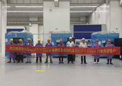
Jingce Electronics' Seal series TGV testing equipment was successfully delivered in batches to leading customers in the TGV industry in Central China​


Jingce Electronics' Seal series TGV (Through Glass Vias) testing equipment was successfully delivered in batches to a leading customer in the TGV industry in Central China . This is the first time that the Seal series TGV testing equipment independently developed by Jingce Electronics has been successfully delivered in batches in the TGV field, marking another important breakthrough for Jingce Electronics in the field of semiconductor FOPLP advanced packaging testing.

This leading customer uses the company's independently developed TGV technology (through glass via interconnection technology) in Mini/Micro LED direct display, semiconductor advanced packaging substrates and other precision device fields. Its TGV technology capabilities and production capacity layout are in the leading position in the industry.

Driven by multiple forces of R&D and production, Jingce Electronics collaborated across multiple departments to successfully develop related products and achieve batch shipments to leading customers in the industry, fully demonstrating Jingce Electronics' outstanding technical strength in testing equipment in the field of semiconductor TGV advanced packaging applications, and also highlighting its strong R&D capabilities, production capabilities and growing market competitiveness.
1731594431805.png

The Seal series TGV inspection equipment independently developed by Jingce Electronics represents the company's latest technological achievements in the field of semiconductor inspection. The Seal series products are mainly used to inspect TGV through holes, metal filling in holes, surface metallization, RDL process and other key process flow inspections. The inspection defects include graphic abnormalities, surface damage, dirt and foreign matter, short circuits, open circuits, scratches, residues, etc. It can be optionally equipped with integrated key dimension measurement and film thickness measurement function modules. The equipment has high inspection accuracy and excellent data processing capabilities. It can accurately capture defects in fine structures and provide detailed inspection reports to help customers improve production efficiency and product quality. The TGV inspection machine equipment software is fully independently developed with independent intellectual property rights. Combined with Jingce Electronics' many years of technical experience in the field of quality inspection, it promotes the localization and application of TGV inspection equipment.

Please, Log in or Register to view URLs content!
 

tokenanalyst

Brigadier
Registered Member
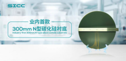
The industry's first 300mm N-Type silicon carbide substrate

1731594730095.png


With the rapid development of new energy vehicles, clean energy such as photovoltaic energy storage, 5G communications, and high-voltage smart grids, the demand for silicon carbide-based devices that meet high-power, high-voltage, and high-frequency working conditions has also grown dramatically. 300mm silicon carbide substrate materials can further expand the area available for chip manufacturing on a single wafer, greatly increasing the output of qualified chips. Under the same production conditions, the output can be significantly increased, the unit cost can be reduced, and the economic benefits can be further improved, providing the possibility for a larger-scale application of silicon carbide materials.

By adding 300mm silicon carbide substrate products, Tianyue Advanced has created more differentiated product lines and met the diverse needs of customers in terms of product quality and performance. The launch of this product responds to the market's urgent demand for high-performance silicon carbide materials, reflects the company's continued investment in technological innovation and product upgrades, and is a forward-looking layout for future market trends.

Please, Log in or Register to view URLs content!
 

tphuang

Lieutenant General
Staff member
Super Moderator
VIP Professional
Registered Member
The industry's first 300mm N-Type silicon carbide substrate

View attachment 139359


With the rapid development of new energy vehicles, clean energy such as photovoltaic energy storage, 5G communications, and high-voltage smart grids, the demand for silicon carbide-based devices that meet high-power, high-voltage, and high-frequency working conditions has also grown dramatically. 300mm silicon carbide substrate materials can further expand the area available for chip manufacturing on a single wafer, greatly increasing the output of qualified chips. Under the same production conditions, the output can be significantly increased, the unit cost can be reduced, and the economic benefits can be further improved, providing the possibility for a larger-scale application of silicon carbide materials.

By adding 300mm silicon carbide substrate products, Tianyue Advanced has created more differentiated product lines and met the diverse needs of customers in terms of product quality and performance. The launch of this product responds to the market's urgent demand for high-performance silicon carbide materials, reflects the company's continued investment in technological innovation and product upgrades, and is a forward-looking layout for future market trends.

Please, Log in or Register to view URLs content!
yeah, I just saw this too, pretty big deal for SICC to hit this mark.

Please, Log in or Register to view URLs content!

Wolfspeed got no tech advantage after this.
 

broadsword

Brigadier
China has successfully developed a key technology for the manufacturing of trench-type silicon carbide (SiC) MOSFET chip This is nine years after Rohm started manufacturing the world's first trench-type silicon carbide (SiC) MOSFET chip. Less current resistance is its benefit.


Nanjing, China Achieved Breakthrough in Manufacturing Key SiC Chip for the First Time​


2024-09-03
Please, Log in or Register to view URLs content!
editor

News
20240902152600_640-4-624x253.png

As per
Please, Log in or Register to view URLs content!
, the National Third-Generation Semiconductor Technology Innovation Center (Nanjing) has successfully developed a key technology for the manufacturing of trench-type silicon carbide (SiC) MOSFET chip after four years of independent research. This breakthrough surpasses the performance limitations of planar SiC MOSFET chip, marking the first achievement of its kind in China.

SiC is one of the main representatives of wide bandgap semiconductor materials, characterized by its wide bandgap, high critical breakdown electric field, high electron saturation velocity, and high thermal conductivity. SiC MOSFET primarily comes in two structures: planar and trench, predominantly the former in current SiC MOSFET chip field.

Planar SiC MOS structure features simple process, good cell consistency, and relatively high avalanche energy. However, it faces the issue of JFET effect caused when current is confined to a narrow N-region near the P-body, which increases the on-resistance, and the large parasitic capacitance.

Trench structure refers to embedding the gate into the substrate to form a vertical channel, which allows for increased cell density, elimination of the JFET effect, optimal channel mobility, and significantly reduced on-resistance compared to planar structure. However, the trench process is more complex, with poorer cell consistency and lower avalanche energy.

“The key lies in the process,” explained Huang Runhua, Technical Director at the National Third-Generation Semiconductor Technology Innovation Center (Nanjing).

He noted that SiC is extremely hard, so converting from a planar to a trench structure means “digging a trench” in the material, which must be done with precision to avoid unevenness. During fabrication, the etching process’s precision, etching damage, and residual surface materials critically impact the development and performance of SiC devices.

To address these issues, the Innovation Center organized a core R&D team along with a full support team, and finally established a novel process flow following four years of continuous experimentation with new processes.

They overcame the challenges of precise, stable trench etching and successfully manufactured trench-type SiC MOSFET chip, improving conduction performance by about 30% compared to planar type.

The center is currently developing trench-type SiC MOSFET chip, with the goal of launching trench-type SiC power devices within a year, which are expected to be introduced to applications such as electric vehicle drivetrains, smart grids, photovoltaic energy storage.

What impact does this breakthrough have on our lives and the semiconductor industry? Huang explained, using electric vehicle as an example, that SiC power devices inherently offer power-saving advantages over silicon devices, potentially increasing lifespan by about 5%, and trench structure allows for designs with even lower resistance.

With the same conduction performance, this enables a higher-density chip layout, reducing chip usage costs.

Now, the National Third-Generation Semiconductor Technology Innovation Center (Nanjing) has already started research on SiC superjunction devices. “This structure outperforms the trench-type structure and is currently under development,” Huang Runhua revealed.
 

tonyget

Senior Member
Registered Member
I'm kind of curious,is Huawei's Ascend the only domestic AI chip player?What happened to other domestic AI chip player?

I mean,there was alot of buzz around domestic AI chips,we can always see related news every onces in a while. But in the end,it seems that only Huawei's Ascend get mass produced and adopted
 

tokenanalyst

Brigadier
Registered Member

Kema Technology leads the new wave of semiconductor equipment industry chain​

Suzhou Kema Materials Technology Co., Ltd. has become a leading domestic company in advanced ceramic materials and components based on its full understanding of technology and continuous investment in equipment. It has also become one of the few domestic companies that has mastered the core technology of the entire process of advanced ceramic components for semiconductor equipment from material formulation to component manufacturing and has achieved large-scale overseas sales.
Recently, Kema Technology released its 2024 third quarter report, which is also its first third quarter report since its listing. The report shows that the company's operating income in the first three quarters was 616 million yuan, a year-on-year increase of 74.65 %; net profit attributable to the parent was 226 million yuan, a year-on-year increase of 295.42%; net profit attributable to the parent after deducting non-recurring items was 220 million yuan; basic earnings per share was 0.61 yuan.

In terms of a single quarter, Kema Technology achieved total operating revenue of 232 million yuan in the third quarter, a year-on-year increase of 95.11%; net profit attributable to shareholders of the parent was 86.6613 million yuan, a year-on -year increase of 275.56%.

When talking about the reasons for the significant increase in revenue and net profit in the first three quarters, Kema Technology pointed out that, first, thanks to the recovery of global semiconductor capital expenditure and the increase in downstream demand, the market demand for advanced ceramic components made of alumina materials used in the company's traditional business in the pan-semiconductor field has increased significantly compared with the same period last year, and the company has delivered a large number of such products; second, the company's semiconductor equipment core components, ceramic heaters, have achieved domestic substitution. This type of product solves the "bottleneck" problem of key components of CVD equipment of downstream wafer manufacturers. Downstream customers have strong demand for such products, generating higher profits.

From the first three quarters of 2024, the two products of advanced ceramic components and ceramic heaters used in the pan-semiconductor field accounted for approximately 80% of the company's operating income, which is the company's main source of income.

Looking at the revenue data of previous years, Kema Technology's performance is still stable. From 2021 to 2023, Kema Technology's main business income is mainly from the sales revenue of advanced ceramic material components and pan-semiconductor equipment surface treatment service revenue, and the revenue shows a year-on-year growth trend, with operating income of 345 million yuan, 462 million yuan and 480 million yuan respectively, with a three-year compound growth rate of 18.01%; the net profit attributable to the parent company is 67.0888 million yuan, 93.2362 million yuan and 81.8607 million yuan respectively, all maintained at a high level.

Please, Log in or Register to view URLs content!
 
Top