Chinese semiconductor thread II

tphuang

Lieutenant General
Staff member
Super Moderator
VIP Professional
Registered Member
If no Chinese company has access to TSMC any more, what's the reason to allow TSMC to keep operating.

I think sabotage on TSMC advanced ( 7nm<= ) foundries is now a viable and acceptable action per game theory.

Basically, if I cannot have them, I will at least make sure you cannot have them as well
so this is only for AI chips. I assume they will still get other chips fab'd at TSMC.

oh I think I misread. If it's for Chinese AI makers only and not for all Chinese companies then I take it back. In that case, the game theory calculation needs to be closely looked at

If it was all Chinese companies, no need for calculation, sabotage is the only viable action remaining
I think longer term, this will expand. And it will be a good thing if that expands, since Chinese chipmakers won't have to deal with TSMC competition.
AI for automotive, i.e. ADAS is a key strategic technology with huge market potential within the end of this decade. Now Horizon Robotics will get a hit. It is critical for China do not let the ADAS train move on without China is onboard....
Well, if Horizon had any sense, it would have received a million chip by this point for J6. They basically use N6, which is something that works quite well with SMIC's N+3 process. As long as SMIC can ramp up production.
 

tphuang

Lieutenant General
Staff member
Super Moderator
VIP Professional
Registered Member
Sales up 34% YoY. Nothing short of amazing.
Another 21k wpm in a single quarter. That would be close to a gigafab in a single year.
90.4% utilization rate. So much for overcapacity.

It is not surprising that capex is going down. They likely finished construction of all the buildings at this stage. Probably started moving tools in early this year already. They will be filling those buildings with tools before expanding again. Maybe next year or the year after that.
Look at below, 50k wpm in half a year. That's crazily high.

For interested people, here are the official documents from SMIC

Please, Log in or Register to view URLs content!

Please, Log in or Register to view URLs content!

Some noteworthy point:

- 86% of revenues from China, while just 10% from US. These are records high and low respectively.

- Capacity reached 884K wpm (8" equivalent), almost +90K wpm since 1 year ago and a whopping +47K wpm in just one quarter! New stuff is finally coming online now!

- Big drop of capital expenditure compared to previous quarters: 2.25B$ -> 1.18B$
yeah, and the pace is expanding. I would assume the decreased capex is because they were stocking up heavily in first half of the year while new sanctions have yet to enter into place.
Will add another 30k wpm in fourth quarter.

Please, Log in or Register to view URLs content!
在晶圆尺寸结构方面,中芯国际12英寸产线产能已经接近满载,且有新开出的产能迅速验证并投入生产,收入占比快速提升至78.5%;8英寸产线收入占比下降至21.5%,但由于BCD需求持续良好,会推动8英寸产线产能利用率的上升。

此外,中芯国际给出2024年第四季度指引,营收环比持平到增长2%,毛利率介于18%至20%之间。管理层给出此判断主要是基于,中芯国际12英寸产能在过往多个季度持续供不应求,一些客户的订单只能延期完成;中芯国际在第四季度会进一步释放3万片12英寸月产能。在多重积极因素推动下,中芯国际将做到环比持平或略有增长。

This is very interesting. 12-inch demand is just insatiable from local customers. They are adding 50k wpm in half a year. That's insanely high

在下游应用领域方面,智能手机、电脑与平板、消费电子、互联与可穿戴、工业与汽车占比分别为25%、16%、43%、8%和8%。消费类是仍然是中芯国际收入占比最大的应用分类,消费类市场整体需求正在逐步恢复,消费产品功能升级落地,并对出口保有良好需求。
in terms of downstream demand. smart phones 25%, flat screen computer/computer 16%, consumer electronics 43%, IoT 8% and auto 8%. Good news for domestic manufacturers to achieve supply chain security.
 

huemens

Junior Member
Registered Member
Look at below, 50k wpm in half a year. That's crazily high.

Just to add a little more clarity, the 47k number for the quarter is in 8-inch equivalent units. The actual capacity added last quarter was 21k in 12-inch. From the report
12-inch monthly capacity increased by 21 thousand wafers
Monthly capacity increased to 884,250 8’ equivalent wafers in 3Q24 from 837,000 8’ equivalent wafers in 2Q24.

Increase so far this year (in 8-inch equivalent):
Q1: 9k
Q2: 22.5k
Q3: 47.25k

Total 35k in 12-inch
 
Last edited:

gelgoog

Lieutenant General
Registered Member
TSMC Reportedly to Halt 7nm and Below Chip Shipments to China’s AI Firms Next Week
Please, Log in or Register to view URLs content!
Maybe China should stop exporting neon gas to Taiwan.

AI for automotive, i.e. ADAS is a key strategic technology with huge market potential within the end of this decade. Now Horizon Robotics will get a hit. It is critical for China do not let the ADAS train move on without China is onboard....
I expected this much to happen. Companies like Horizon Robotics are really dumb by putting all their eggs in the TSMC basket.
 
Last edited:

tokenanalyst

Brigadier
Registered Member

All the domestic chip designers have probably been expecting this. If they haven't been working with SMIC, they deserve whatever they are getting.
Losing Chinese AI clients will likely to stress out TSMC advance nodes. One the reason why Samsung EUV nodes are doing so poorly is the lack of AI clients who a lot of them come from China.
 

tokenanalyst

Brigadier
Registered Member

Shengmei Shanghai's front-end semiconductor manufacturing cleaning equipment Ultra C Tahoe has achieved important performance breakthroughs​


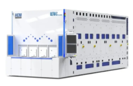
ACM Semiconductor Equipment (Shanghai) Co., Ltd. (hereinafter referred to as "ACM Shanghai") (Sci-Tech Innovation Board Stock Code: 688082), as a leading supplier of wafer process solutions for semiconductor front-end and advanced wafer-level packaging applications, today announced that its cleaning equipment product Ultra C Tahoe has achieved an important performance breakthrough. This upgrade can meet the stringent technical requirements of more advanced wafer foundry, logic devices and memory devices.

Ultra CTahoe's patented hybrid architecture is the first to combine a tank cleaning module and a single wafer cleaning chamber into the same SPM equipment. This architecture has stronger cleaning performance, higher production capacity and better process flexibility. In the medium and low temperature sulfuric acid (SPM) cleaning process, UltraCTahoe can achieve the effect of an independent single wafer cleaning equipment and reduce chemical consumption by up to 75%. According to Shanghai Shengmei's estimates, sulfuric acid alone can save up to $500,000 per year, and the treatment of sulfuric acid waste can further reduce costs and be more environmentally friendly.

Dr. Wang Hui, Chairman of Shengmei Shanghai, said: “As artificial intelligence continues to move closer to consumers’ lives, we expect the public to pay more and more attention to the impact of semiconductor chip manufacturing on environmental pollution.

We believe that SCM Shanghai's UltraCTahoe can help customers increase the production of advanced AI chips while reducing environmental impact. SCM Shanghai has a creative R&D team, and UltraCTahoe once again witnessed the team's excellent performance. We believe that the Tahoe platform is fully capable of occupying an important position in the SPM medium and low temperature application field, which accounts for about 20% of the entire cleaning market.
1731076839578.png

New features and benefits of the upgraded UltraCTahoe:

1. Stronger particle removal performance: The Tahoe platform has strong cleaning capabilities, achieving an average particle count of less than 6 in the 26nm particle test, which can meet the stringent requirements of advanced node manufacturing. In the future, the equipment will add a more sophisticated particle filtration system that can remove 1x nanometer particles, which can be used for cutting-edge logic and memory applications.
2. Higher capacity: The upgraded 25-slot slot module (previously 13 slots) and 9 single-wafer chambers (previously 8 chambers) have an hourly capacity of more than 200 wafers, which can be compared with the 12-cavity comparable to SPM system.
3. Better cost control and environmental protection level: UltraCTahoe can reduce sulfuric acid consumption by up to 75%, thereby reducing large-scale manufacturing costs and meeting increasingly stringent environmental regulations to achieve sustainable development goals.
4. Wider process applications: 30+ production layers have been certified, including key production processes such as lightly doped drain (LDD) and source/drain (SD), and more layers and applications are under development.
5. More flexible single wafer cleaning applications: Optional configurations include new spray technology, ACM Shanghai’s patented SAPS/TEBO technology and HOTIPA drying technology, which improves the versatility of the equipment in a variety of process applications.

Please, Log in or Register to view URLs content!
 

tphuang

Lieutenant General
Staff member
Super Moderator
VIP Professional
Registered Member
Just to add a little more clarity, the 47k number for the quarter is in 8-inch equivalent units. The actual capacity added last quarter was 21k in 12-inch. From the report


Increase so far this year (in 8-inch equivalent):
Q1: 9k
Q2: 22.5k
Q3: 47.25k

Total 35k in 12-inch
I said 50k in half a year.
Q3 added 21k and they are projecting to add 30k in Q4. Why are you using 1 quarter of 8-inch equivalent to compare?

Maybe China should stop exporting neon gas to Taiwan.


I expected this much to happen. Companies like Horizon Robotics are really dumb by putting all their eggs in the TSMC basket.
It's fine. Horizon was wise to do it on 6nm process which it can replicate on SMIC. It's players like NIO and XPeng that are screwed. Besides, Horizon probably got enough samples now that it has delivered to customers already.
 

tokenanalyst

Brigadier
Registered Member

Characterization of optical depth for laser produced plasma extreme ultraviolet source​

SIOM​

Abstract​

This study investigates the emission mechanism of laser-produced plasma extreme ultraviolet source (LPP-EUV). In the experiment, the EUV radiation is generated by a 1064 nm laser interacting with slab Sn target. The EUV emission is characterized by EUV energy monitors and an EUV spectrometer. The dependency of CE on laser intensity and plasma relative optical depth is explored by a plasma emission-absorption layer model. The dependency is confirmed by an optical interferometry measurement of plasma electron density for the first time. Our work provides a method for characterizing and optimizing the optical depth of laser driven EUV source.

Experimental setup​

The experimental layout of the laser interacting with the slab Sn target is shown in Fig. 1. A 1064 nm Nd: YAG drive laser is focused by a convex lens (F = 400 mm) onto the target at normal incidence. The Sn target is mounted in a vacuum chamber, which is pumped to 10−5Pa. After each laser shot, the target is moved to a fresh surface to guarantee identical laser-target interaction. The FWHM pulse width τ0 of the drive laser is 4.8 ns. The laser energy ranges from 4 mJ to 170 mJ with an FWHM​

Results and discussion​

The dependency of the EUV spectrum on laser intensity is shown in Fig. 3(a). The laser is kept at best focus on the target. The laser peak intensity is varied by changing laser energy. The EUV spectrum is normalized to the laser energy. In-band EUV emission grows rapidly and reaches a peak at 5.2×10¹¹W/cm2, then decreases slightly as laser intensity further increases to 1.8×10¹²W/cm2. This tendency agrees well with the results measured by the EUV energy monitors.​

Conclusions​

EUV in-band emission is characterized at different angles relative to the drive laser direction. An emission-absorption layer model is proposed to explain the difference between emission angles and the dependency on laser intensity, which shows that the optical depth is crucial to the total EUV emission. Plasma scale lengths deduced from electron density measurements representing relative optical depth are consistent with the theoretical model.​

Please, Log in or Register to view URLs content!
 
Top