Chinese semiconductor thread II

tokenanalyst

Brigadier
Registered Member

Domestic 8-inch visual SiC resistance furnace debuts!​


The 8-inch resistance-method silicon carbide single crystal furnace developed by Jingsheng Co., Ltd. can make the silicon carbide crystal growth process "visible", thereby reducing R&D costs and providing an equipment foundation for the mass production of 8-inch substrates.

According to Wu Chunsheng, secretary of the board of directors of Jingsheng Co., Ltd., the growth of silicon carbide single crystals was previously carried out in a completely closed "black box". The growth process was not visible, so each time you looked at the crystal, it was like opening a " blind box " . Only when you opened the furnace body could you know the growth status of the crystal. Due to the lack of effective means of observing the growth status of the crystal, abnormalities in the crystal growth process could not be adjusted in time, and process development required a lot of experiments for trial and error and iterative optimization, which led to problems such as long development cycle, high cost, and low yield.

The 8-inch resistance method silicon carbide single crystal furnace launched by Jingsheng Co., Ltd. introduces a visual detection system , which can make the crystal growth process visible. Wu Chunsheng further introduced that based on real-time observation of growth rate and powder evolution state, the single crystal furnace can adjust power, pressure and other conditions through intervention to keep crystal growth in a controllable state.

In addition, to address the difficulty of temperature gradient control, the equipment adopts a multi-heater layout , and each heater can be controlled individually, which effectively solves the problem of poor controllability of temperature gradient and improves the quality of crystal growth. The Jingsheng team conducted dozens of experiments in simulation, structure, and material selection, and finally found the balance between the two, reducing the minimum crystal growth power from 30kW~40kW to below 25kW .

Please, Log in or Register to view URLs content!
 

tokenanalyst

Brigadier
Registered Member

Gallium Semiconductor successfully prepared 2-inch gallium oxide single crystal using VB method (non-iridium crucible).​


Hangzhou Gallium Ren Semiconductor Co., Ltd. (hereinafter referred to as Gallium Ren Semiconductor) achieved a new technological breakthrough in the growth of gallium oxide crystals. Based on the independently developed gallium oxide dedicated crystal growth equipment (non-iridium crucible), it successfully grew a 2-inch gallium oxide single crystal using the vertical Bridgman method (VB), which is the first time in China.​

1730133676590.png1730133697159.png

Please, Log in or Register to view URLs content!
 

tokenanalyst

Brigadier
Registered Member

Gallium oxide dedicated crystal growth equipment​


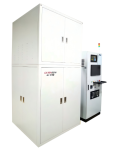
Hangzhou Gallium Semiconductor Co., Ltd. (hereinafter referred to as "Gallium Semiconductor"), as a pioneer in the field of ultra-wide bandgap semiconductor gallium oxide materials , released the company's first gallium oxide dedicated crystal growth equipment. This equipment not only meets the various requirements of gallium oxide crystal growth, but also integrates a number of independent innovative technologies. It is a new milestone for Gallium Semiconductor to achieve a closed loop of gallium oxide single crystal material technology. The gallium oxide crystal growth equipment launched by Gallium Ren Semiconductor this time meets the high temperature and high oxygen environment required for gallium oxide growth. The equipment uses non-iridium ( Ir ) crucible materials and can work in an air atmosphere. The R&D team independently designed a unique composite temperature measurement technology and temperature control algorithm to ensure the stability, uniformity and consistency of the crystal growth process. The equipment realizes a fully automated crystal growth process, reduces manual intervention, and significantly improves production efficiency and crystal quality. The gallium oxide crystals prepared by this equipment are columnar in shape. Through process control, large-sized single crystals with various crystal faces can be obtained, and it supports the upgrade to larger single crystals to adapt to the evolving epitaxial technology and device requirements. Gallium Ren Semiconductor can also provide growth process files for multiple crystal faces to achieve highly personalized product customization to meet the scientific research, production and other needs of universities, research institutes and corporate customers for gallium oxide crystal growth.

1730134080897.png

Please, Log in or Register to view URLs content!
 

tokenanalyst

Brigadier
Registered Member

SMIC's Q3 revenue increased by more than 27%, and its gross profit margin turned positive to 6.16%​


On the evening of October 28, Xinlian Integrated Circuit released its third quarter report for 2024. In the third quarter of 2024, the company achieved a single-quarter revenue of 1.668 billion, a year-on-year increase of 27.16%; the gross profit margin turned positive to 6.16%, an increase of 14.42 percentage points year-on-year.
Driven by the good performance in the third quarter, Xinlian Integrated's cumulative operating income in the first three quarters reached 4.547 billion, an increase of 18.68% year-on-year; the net profit attributable to the parent was -684 million yuan, a year-on-year reduction of 677 million yuan, and the loss margin decreased by 49.73%; EBITDA (earnings before interest, taxes, depreciation and amortization) was 1.660 billion yuan, an increase of 798 million yuan year-on-year, an increase of 92.65%.
Power revenue grew strongly and is expected to continue to improve in the fourth quarter
Benefiting from the recovery of the new energy vehicle and consumer markets, the company's capacity utilization rate increased steadily in the third quarter, and the scale effect gradually emerged, driving a rapid increase in operating income. Among them, the revenue of the new energy vehicle business segment increased by nearly 30% year-on-year, and the revenue of the consumer sector increased by nearly 90% year-on-year.
At present, the company's related technical products have been designated for purchase by many well-known vehicle manufacturers such as BYD, Xpeng, NIO, Ideal, GAC Aion, etc., and have successfully entered overseas markets such as Europe, and have been mass-produced by well-known European car companies and many overseas Tier 1 companies.
According to the installed capacity of power modules for passenger cars in China in the first three quarters of 2024 released by NE Times, the installed capacity of Xinlian integrated power modules has exceeded 910,000 sets, with a year-on-year growth rate of more than 5 times.

Please, Log in or Register to view URLs content!
 

tokenanalyst

Brigadier
Registered Member

Prototype optical enhancement cavity for steady-state microbunching​


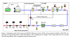
The innovative mechanism of steady-state microbunching (SSMB) promises a potent light source, featuring high repetition rate and coherent radiation. The laser modulator, comprising an undulator and an optical enhancement cavity, is pivotal in SSMB. A high-finesse prototype optical enhancement cavity for SSMB with an average power of 55 kW is described in this paper. Preliminary design of the laser modulator, experimental setup, and methods to address frequency degeneracy and power coupling issues are discussed. D-shaped mirrors are utilized to successfully suppress the modal instability. This study is the first to illustrate the finesse reduction caused by high-order mode damping during experiments. The experimental and simulation results match closely. A cavity power coupling model is established, and the experimental results verify the correctness of the coupling model. A method for estimating the absorption coefficient through thermal-induced evolution of cavity mode has been implemented. Experimental results demonstrate a high-average-power enhancement cavity with a finesse of 16 518 ± 103 and an estimated average absorption coefficient of 12 ppm for the cavity mirrors. The findings contribute to the advancement of SSMB by providing insights into the design and operation of high-power optical enhancement cavities.

Please, Log in or Register to view URLs content!
 

GulfLander

Senior Member
Registered Member
"Intel to expand Chengdu facility, despite US China tension
Chipzilla unlikely to give in when it comes to its biggest sales market
Intel is expanding its packaging and testing base in Chengdu, a move that signals its intent to remain firmly rooted in the Chinese market, despite geopolitical pressures.

Chipzilla confirmed via social media on Monday morning that relevant planning and construction has already begun on the 21-year-old facility.

The expansion will introduce packaging and testing services for server chips and establish a "customer solutions" center that promotes digital transformation and "provides customized solutions based on Intel architecture and products to industry."
"The expansion plan reflects Intel's continued cultivation and development in Chengdu," explained Intel.

Wang Rui, chairman of Intel China, said "China's continuous promotion of high-quality development and high-level opening up to the outside world are the foundation and driving force for Intel's long-term development in the Chinese market."

China was Intel's largest sector last year, accounting for 27 percent of its $54 billion revenue in 2023.

Beijing however, doesn't appear to be as keen on Intel's affinity and would prefer homegrown chips to those from western companies. In April, China's Ministry of Industry and Information Technology told domestic telcos to inspect and make a plan to remove non-Chinese semiconductors from their networks, a move that largely impacted Intel, along with AMD.

This move was perceived as retaliatory, especially in light of the U.S. Federal Communications Commission's earlier ban on Huawei and ZTE telecommunications equipment in the US market.
Intel CEO Pat Gelsinger has been vocal about his disdain for US export restrictions on China, but they've sparked no change. Further regulations from the Biden Administration, were issued just this past summer, including ones with great effect on Intel's investment arm.

Overall, Intel has not been having an easy time. It's Q2 earnings report was largely considered disastrous and included news of $1.6 billion in net losses, a 15 percent global workforce cut and reduced capital expenditures.

Soon after, Gelsinger announced it would be spinning out its Foundry division as an independent subsidiary.

Meanwhile, the tit-for-tat drama between China and the US with Intel in the middle carried on. Chipzilla was accused by an industry group of putting backdoors into its China chips at the direction of America's NSA. In response, Intel promised it follows the law everywhere it does business.

Intel would like to very much stay on the good side of both governments, especially while the US is doling out CHIPS subsidies for domestic fab expansions.

Intel was awarded $8.5 billion in grants and $11 billion in loans in March under the Chips and Science Act. It reportedly qualified for another $3.5 billion in federal grants to make semiconductors for the Pentagon last month. " theregister

Please, Log in or Register to view URLs content!

Please, Log in or Register to view URLs content!
 

gelgoog

Lieutenant General
Registered Member
Intel is expanding its packaging and testing base in Chengdu, a move that signals its intent to remain firmly rooted in the Chinese market, despite geopolitical pressures.

Chipzilla confirmed via social media on Monday morning that relevant planning and construction has already begun on the 21-year-old facility.
What a load of bull. Intel dumped their NAND fab at Dalian onto SK Hynix. Intel closed their R&D labs in China. And then the US government started sanctioning fabs in China left and right a couple years later. Intel clearly had advance warning from the US government they were going to turn the screws on China. SK Hynix were burned with US policy on no upgrades to their memory fabs in China and eventually the South Korean government convinced the US government to at least allow upgrades of tools already in the fabs. Probably as a condition for Samsung to build their latest fab in Texas.

This move by Intel to expand a packaging facility in China is similar to what Micron did after they got hit by counter-sanctions by the Chinese government. They would have never even considered that pitiful investment if they didn't stand to lose hugely more from the Chinese government's counter-sanctions. A mere token gesture. They would lose hundreds of billions in sales, so they will invest hundreds of millions.

Hopefully the Chinese semi tools sector will be able to make all the tools for chips soon and completely displace Western vendors.
 
Last edited:
Top