Chinese semiconductor thread II

huemens

Junior Member
Registered Member

U.S. Reportedly Investigates TSMC on whether It Manufactured AI or Smartphone Chips for Huawei​

Please, Log in or Register to view URLs content!
The ongoing investigation is examining whether TSMC has been engaged in the production of AI chips designed by Huawei, according to the report. These AI server chips have gained popularity among Chinese customers as an alternative to NVIDIA’s chips, which they are barred from purchasing due to U.S. export regulations.
Additionally, the inquiry is said to be exploring whether TSMC manufactured smartphone chips for Huawei’s devices as well. The Information notes that Huawei’s Mate 60 series, featuring a processor made in China by SMIC, was a potential target of investigation.

TSMC says it is a law abiding company, after report of US probe​

Please, Log in or Register to view URLs content!
 

ansy1968

Brigadier
Registered Member

U.S. Reportedly Investigates TSMC on whether It Manufactured AI or Smartphone Chips for Huawei​

Please, Log in or Register to view URLs content!


TSMC says it is a law abiding company, after report of US probe​

Please, Log in or Register to view URLs content!
Simply Extortion, just like a mafia boss, nothing is free that includes your mother , wife and children, dependency is a two edge sword either you comply or be taken over there is NO MIDDLE GROUND when dealing with this people.
 

tokenanalyst

Brigadier
Registered Member

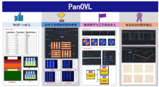
Oriental Crystal Source PanGen platform adds a new member, PanOVL, the marking optimization tool, is launched​


When the semiconductor manufacturing process evolves to the 22nm node and below, with the introduction of multiple patterning technology, the requirements for overlay errors between different process layers become increasingly higher. Overlay measurement technology can be divided into image plane image recognition measurement technology and diffraction-based DBO (Diffraction Based Overlay) measurement technology. Compared with the image recognition-based method, diffraction-based overlay error measurement has better measurement result repeatability, lower device-induced measurement error TIS (Tool Introduced Shift), and can adapt to smaller feature sizes. It has become a widely used overlay measurement method for large-scale integrated circuits at the 22nm and below process technology nodes.

In order to measure the overlay error, a specific overlay mark needs to be specially designed on the wafer. The performance of the overlay error device measurement depends largely on the design of the overlay mark. The DBO overlay mark optimization tool based on computational lithography can simulate the key indicators of overlay error measurement, so that a better overlay mark design scheme can be given based on the simulation results, thereby shortening the mark development cycle and improving the efficiency and quality of the entire lithography process.

Based on the solid computational lithography platform PanGen®, Oriental Crystal Source launched the DBO overlay mark simulation optimization product PanOVL, which can simulate the overlay mark from multiple key indicator dimensions. At the same time, considering the application scenario of large-scale simulation of massive overlay marks, PanOVL introduced a distributed computing framework, which greatly accelerated the efficiency of finding better overlay marks through simulation.

1729259683593.png

Oriental Crystal Source's PanOVL software uses the PanGen OPC ® engine and the PanGen Sim ® rigorous electromagnetic field simulation engine, with the help of the GPU+CPU hybrid computing platform and the PanGen ® distributed computing framework, to perform large-scale overlay mark simulation, and integrate the simulation results of multiple dimensions to select the overlay mark scheme with better performance for actual lithography.
PanOVL can identify overlay marks with a large process window, give overlay marks that meet good signal-to-noise ratios and have stronger detection signal resistance to process disturbances, and can also simulate the impact of exposure process aberrations on overlay marks, providing overlay marks that make overlay measurement results more in line with the actual device situation.

Please, Log in or Register to view URLs content!
 

tokenanalyst

Brigadier
Registered Member
FORTY years building a brand inside China just to see it all burn because some Social Science grads Think Tank stooges who have never worked in the industry want to push their careers inside the DoD.


Applied Materials China holds headquarters celebration ceremony to celebrate 40th anniversary in China​

October 18 , 2024 , Shanghai - In 2024 , Applied Materials will celebrate its 40th anniversary in China. As an important milestone in its 40 years of development in China, Applied Materials held the "Applied Materials China Headquarters Celebration Ceremony" today in Zhangjiang Hi-Tech Park, Pudong New District, Shanghai. Applied Materials President and CEO Gary Dickerson, global management executives, Applied Materials Vice President and Applied Materials China President Yao Gongda, as well as leaders and industry partners from all walks of life such as the Shanghai Integrated Circuit Industry Association and Shanghai Zhangjiang Hi-Tech Park Development Co., Ltd. witnessed the celebration ceremony.
Applied Materials is the first international semiconductor equipment company to enter China. At the celebration ceremony, Applied Materials reviewed the important business milestones since the opening of the Customer Service Support Center in Beijing in 1984 , showing Applied Materials' 40 years of cooperation with domestic and foreign customers and partners, as well as its support for the sustainable development of the global chip industry.
"The ceremony at our new Shanghai headquarters marks another exciting milestone in Applied Materials' long history in China," said Gongda Yao, vice president of Applied Materials and president of Applied Materials China . "Today is also a moment to celebrate our employees for their dedication and the great work they do for our business and our communities - what makes Applied Materials a great company."

Please, Log in or Register to view URLs content!
 

tokenanalyst

Brigadier
Registered Member

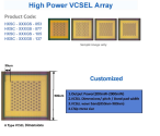
Huaxin Semiconductor's VCSEL chip R&D project was approved​


Recently, the Jiangsu Provincial Department of Science and Technology issued the "Public Notice of Proposed Projects in the Provincial Frontier Technology R&D Plan for 2024", and the R&D project of 112Gbit/s PAM4 VCSEL chip of Jiangyan High-tech Zone enterprise Huaxin Semiconductor Technology Co., Ltd. was approved.

It is reported that VCSEL chips, as vertical cavity surface emitting laser chips, are widely used in Ethernet, data centers, intelligent computing centers and other fields due to their high reliability, high stability and high cost performance. The selection into the provincial frontier technology research and development plan is another important milestone achieved by Huaxin Semiconductor on the road of technological innovation.

The launch of this chip will fill the domestic gap, break the foreign technology blockade of my country in the field of high-end VCSEL chips, and further promote my country's independent innovation capabilities in the field of optoelectronic chips.

According to the information, Huaxin Semiconductor Technology Co., Ltd. has internationally advanced epitaxial metal organic chemical vapor deposition (MOCVD) equipment, chip process equipment and packaging equipment, and is mainly engaged in the research, development and production of cutting-edge compound semiconductor optoelectronic chips and their application products. The company's main products are high-brightness LEDs, blue-green semiconductor laser tubes, vertical cavity surface emission (VCSEL) photonic chips, DFB photonic chips, EML photonic chips and high-brightness semiconductor laser chips.

1729263639195.png

Please, Log in or Register to view URLs content!
 

gelgoog

Lieutenant General
Registered Member
I believe Russia is also increasingly producing more and more Helium from its massive LNG field, the US is far from dominating helium production currently. Qatar is producing more
Please, Log in or Register to view URLs content!
.
Those stats are from when the Russians had like 1 train out of 6 total planned operational at the Amur Gas Processing Plant.

Anyone have more knowledge about this? Can China somehow convert this Arm China a completely Chinese company? If so, does it mean it will "own" Arm v9 ISA too? It will be amazing considering how many billions of devices have Arm ISA embedded in then
The whole idea of ARM China was precisely to insulate Chinese companies from Western sanctions. ARM China was supposed to get irrevocable licenses to ARM IP. Which it then would sublicense to Chinese companies.

I kind of doubt it is possible to license ARM v9 to China. Because of SVE. The US put explicit clauses where chips or technologies that use vector units above a certain bit size aren't allowed to be sold or licensed to either China or Russia.
 

huemens

Junior Member
Registered Member
I kind of doubt it is possible to license ARM v9 to China. Because of SVE. The US put explicit clauses where chips or technologies that use vector units above a certain bit size aren't allowed to be sold or licensed to either China or Russia.

It has been posted here multiple times, public statements made by ARM itself, that ARM technology is not of US origin and they are free to license v9 to china. The small core in Huawei's Kirin 9000s is a v9 core from ARM.
 

antiterror13

Brigadier
Those stats are from when the Russians had like 1 train out of 6 total planned operational at the Amur Gas Processing Plant.


The whole idea of ARM China was precisely to insulate Chinese companies from Western sanctions. ARM China was supposed to get irrevocable licenses to ARM IP. Which it then would sublicense to Chinese companies.

I kind of doubt it is possible to license ARM v9 to China. Because of SVE. The US put explicit clauses where chips or technologies that use vector units above a certain bit size aren't allowed to be sold or licensed to either China or Russia.

These might convince you ... and many similar articles about it since 2021
Please, Log in or Register to view URLs content!

Please, Log in or Register to view URLs content!
 

tokenanalyst

Brigadier
Registered Member

Multiple patterning bi-line/tri-line structure at limiting resolution for 7 nm by negative tone development of ArF immersion lithography​


Abstract​

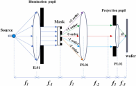
Since the advanced Integrated Circuit (IC) manufacturing process has reached the 14 nm technology node and beyond, the pattern size of integrated circuits has become much smaller than the theoretical minimum resolution of lithography. In order to further extend the performance of immersion lithography, the industry introduces Multiple Patterning Technology (MPT) and Negative Tone Development (NTD) lithography technology. MPT and NTD lithography have greatly improved the process window of immersion lithography, enabling ArF immersion lithography to extend to 7 nm or even 5 nm technology nodes and below. However, MPT still has limited ability to improve the process window for some special patterns. For example,for the poly gate process in Front End of Line (FEOL) or the metal routing process in Back End of Line (BEOL), IC design often uses a special kind of patterns, such as the bi-line or tri-line structures. Due to the fact that some type of the bi-line/tri-line structures have a semi-dense pattern on each side, the process window of these patterns are relatively narrow, making them difficult to manufacture. This paper focuses on the patterning technology scheme of bi-line/tri-line structures in IC design under the diffraction limit of 193 nm immersion lithography. This paper explores the solution for bi-line/tri-line patterns through mask split strategy and NTD lithography process simulation with a physical model, including illumination conditions, Optical Proximity Correction (OPC) methods, and photoresist process parameter design. This study provides a reference scheme for subsequent NTD process development and patterning technology, as well as a reference idea for IC design methods.​

1729289731114.png
1729289822300.png
Please, Log in or Register to view URLs content!
 

gelgoog

Lieutenant General
Registered Member
Those stats are from when the Russians had like 1 train out of 6 total planned operational at the Amur Gas Processing Plant.
Continuing from where I left off,
Please, Log in or Register to view URLs content!

"One of the main products of the Amur GPP is helium, a particularly sought-after element for high-tech industries. With an annual output of 60 million cubic meters, the GPP is poised to become the global leader in helium production. The key link in the logistics chain of helium supplies to the international market will be the helium HUB near Vladivostok, which is going to be put in operation in the nearest future."

That would make the Russians tied with Qatar for helium production in 2023. I have also heard of other proposed helium capture operations in Russia. But those are pretty far away from being into construction yet.

It has been posted here multiple times, public statements made by ARM itself, that ARM technology is not of US origin and they are free to license v9 to china. The small core in Huawei's Kirin 9000s is a v9 core from ARM.
Please, Log in or Register to view URLs content!

"Instruction set: ARMv8.2-A"

Notice how it has NEON but not SVE.

"Each core features a single 128-bit NEON unit. It is capable of executing single double-precision FMA vector instruction per cycle or two single-precision vector instructions per cycle. Operating at 2 GHz, a 64-core chip will have a peak compute of 512 GigaFLOPS of double-precision floating point. It's worth noting that compared to the TaiShan v100, the throughput for single-precision vector has been doubled from 1 to 2 instructions per cycle."

So only 128-bit wide vector instructions.

They could also have cut SVE support for die space reasons. But it seems they currently do not have it.
 
Last edited:
Top