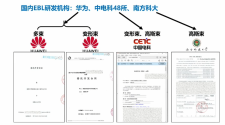
there are plenty of research in EBL and related techs from different companies as well .. accelerate in last 2 years
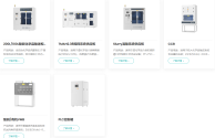
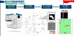
DJEL: the key to the advancement of integrated circuit manufacturing process is the accelerated rise of domestic electron beam measurement equipment
--------------------------------------------------------------------
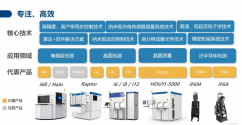
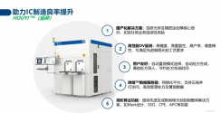
CD-SEM is an advanced fully automatic wafer online measurement equipment. It uses electron beam scanning imaging technology to monitor key process parameters during wafer manufacturing. It is used to measure the critical dimensions of photoresist after development and the contact hole diameter/through hole diameter and gate line width after etching. It is a key device to improve chip manufacturing yield and maintain product quality consistency. Huiran Microelectronics has mastered the underlying design capabilities and independently designed the electronic optical system, image processing algorithm, and high-speed wafer transmission system, providing important microscopic data for the multi-layer and complex integrated circuits.
Huiran Microelectronics stated that overcoming the "bottleneck project" requires unity of purpose. Huiran Microelectronics will work together with customers, suppliers, and partners to continue to overcome key technical difficulties such as electron beam stability and resolution, precise positioning and control, image enhancement and analysis, and improving measurement speed. It will accelerate product iteration, provide more high-performance and reliable options for the integrated circuit industry, and contribute its own strength to the industry.
------------------------------------------------------------------------
Iodonium functionalized polystyrene as non-chemically amplified resists for electron beam and extreme ultraviolet lithography
--------------------------------------------------------------------------
Mechanisms of acid generation from ionic photoacid generators for extreme ultraviolet and electron beam lithography
----------------------------------------------------------------------------
Electron beam focusing technology can be achieved by applying an external electric field or magnetic field, and has the characteristics of high resolution, precise control, non-contact processing and wide application range. This technology is widely used in chip manufacturing in the semiconductor industry, nanostructure preparation in the field of nanofabrication, mask production in the photolithography field, and display imaging in the light source field.
As shown in the figure, the research team deposited a layer of electret material silicon nitride (SiN x ) on the surface of the device. The Si³⁺ trap center inside the SiN x electret can capture and stably store electrons. When electrons are emitted to the surface of the device, the device captures the electrons for charging. The charged device surface is negatively charged, thereby achieving a stable focusing effect on subsequent electrons. Different from traditional electron beam focusing schemes, this new electron beam focusing scheme does not require the introduction of additional electrostatic fields or magnetic fields, providing new possibilities for precise control of electron beams and having important application prospects in the field of micro-nano manufacturing.

