You are using an out of date browser. It may not display this or other websites correctly.
You should upgrade or use an alternative browser.
You should upgrade or use an alternative browser.
Chinese semiconductor thread II
- Thread starter vincent
- Start date
big difference: Taiwanese drivers are a security risk too and there is no process moat as they are typically 90-130 nm node, the sole limit is from the designers, and there's several mainland/HK driver design companies already.
as I wrote here, while Chinese fabs face sanctions, American fabs face Wall Street. Not great for America. But SMIC gets to operate and grow in an environment without competition.
Texas Instruments is also being harassed by an activist investor who wants them to stop their move from 200mm wafers to 300mm wafers.
He basically wants to extract their money via dividends instead of letting them invest in fabs.
Wall Street will be the death of industry in the US. Boeing, Intel, and others are examples of this.
Traditionally Intel used to use their older fabs to make Itanium processors or processor chipsets for motherboards. But Itanium is dead, chipsets are outsourced to TSMC. When they did not have a use for older fabs they just sold the tools and used the shells to put the new tools in.
Intel has lousy experience at working as a 3rd party foundry. We will see if they manage to get over this or not.
Focusing on direct write lithography, the second phase of the Xingji Micro Equipment project was capped
The Phase II project of Xingji Micro-Equipment is located at the intersection of Changning Avenue and Chang'an Road. The project is mainly used to deepen the application of direct writing lithography equipment industry, industrialize IC substrates and substrate-like direct writing lithography equipment, and independently develop key subsystems and core components. The total construction area of the Phase II project is 40,397.93 square meters, of which the modern clean workshop is more than 20,000 square meters, which is more than 2.5 times the area of the clean workshop in the current Phase I plant.

The Phase II factory is expected to be completed and put into production in mid-2025. By then, the Phase I and Phase II factories will be integrated into an integrated R&D and production capacity delivery center, providing strong support for the long-term and stable development of Xingji Micro-Equipment in the future.

The Phase II factory is expected to be completed and put into production in mid-2025. By then, the Phase I and Phase II factories will be integrated into an integrated R&D and production capacity delivery center, providing strong support for the long-term and stable development of Xingji Micro-Equipment in the future.
Nexchip is already producing OLED DDICs.big difference: Taiwanese drivers are a security risk too and there is no process moat as they are typically 90-130 nm node, the sole limit is from the designers, and there's several mainland/HK driver design companies already.
OLED DDICs seem to use higher density processes than LCD DDICs. Maybe due to higher screen resolution. Nexchip is already making 40nm OLED DDICs in small batch production and they expect to make 28nm OLED DDICs eventually.
Other companies such as SMIC also fab OLED DDICs for fabless chip companies in China.
Last edited:
AMEC significant increase in R&D spending.
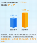
AMEC expects the cumulative new orders in 2024 to reach 11-13 billion yuan. In the first half of the year, AMEC produced a total of 833 cavities of equipment, an increase of about 420% year-on-year, with a corresponding output value of about 6.865 billion yuan, laying a good foundation for shipments and revenue recognition this year.
AMEC's new products continue to gain market recognition, it continues to strengthen its R&D capabilities, accelerate the expansion of its product lines, and significantly increase its R&D efforts to make up for its shortcomings as soon as possible and achieve catch-up. The company's current research projects cover six types of equipment, and more than 20 equipment development projects have been launched and implemented. In the first half of 2024, the company invested 970 million yuan in R&D, a year-on-year increase of 110.84%.
Huaying Micro Equipment was successfully delivered
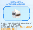
The 12- inch fully automatic metal contamination extraction and detection equipment produced by Wuxi Huaying Microelectronics Technology Co., Ltd. was officially shipped to the top three domestic wafer foundry companies.
As a company committed to technological innovation, Huaying Micro designs, manufactures, and develops new semiconductor manufacturing equipment and new processes with advanced technology, low cost, low resource consumption, and high production efficiency in response to the problems and challenges faced by the semiconductor manufacturing industry. The fully automatic metal contamination extraction and detection equipment delivered this time uses Huaying Micro's original technology "Dynamic Thin Layer DTL Wafer Surface Chemical Treatment Technology", which has many advantages such as strong extraction ability, high extraction efficiency, low method detection limit, comprehensive detection elements, and is not limited by the physical and chemical properties of the wafer surface; it can help chip manufacturers improve pollution detection capabilities and detection efficiency, and speed up the tracing and search of pollution problems.
In the future, Huaying Micro will continue to increase R&D investment, promote technological innovation, and help customers succeed and promote industry development with better products and services. Thank you to all the partners who support and trust Huaying Micro. It is you who make every step of Huaying Micro firm and powerful. Let us look forward to contributing more to the prosperity and development of China's semiconductor industry through continuous technological innovation and win-win cooperation!

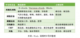
Total investment of about 1 billion yuan for the localization of silicon carbide components for semiconductors.
It is reported that Dezhi New Materials has registered Wuxi Dezhi Semiconductor Materials Co., Ltd. and its subsidiary in Huishan Economic Development Zone. Wuxi Dezhi Semiconductor Materials Co., Ltd. plans to invest a total of about 1 billion yuan to establish 20 integrated circuit epitaxial component production lines and 5 tantalum carbide coating production lines by purchasing highly automated and intelligent production and testing equipment. At the same time, it will build a first-class semiconductor research laboratory and create a research and development and manufacturing base. The project is expected to reach full production within 5 years. As a supporting enterprise, the subsidiary will carry out business simultaneously during the construction of the new base project.


