Chinese semiconductor thread II

PikeCowboy

Junior Member
Power chip is kind of simple.

I think the hardest chip to make for auto is safety brake system and often dominated by Bosch.
next complicated one is battery management chip, for monitor and regulate.
then there's DSP for Motor control.

Does BYD has brake system, battery management and motor control chip? It still has a way to go.
hard like ball point tips or hard like jet engines?
 

tokenanalyst

Brigadier
Registered Member

Microguide Nano: Release of advanced packaging low-temperature thin film deposition system, optimistic about the rapid expansion of the company's ALD & CVD equipment​


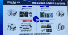
Microguide Nano released its self-developed "Advanced Packaging Low-Temperature Thin Film Application Solution" for the first time at the "16th Integrated Circuit Packaging and Testing Industry Chain Innovation and Development Forum (CIPA2024)".

The solution is designed for the special needs of low-temperature processes for 2.5D and 3D advanced packaging technologies in the semiconductor field, and can achieve high uniformity, high quality, and high reliability thin film deposition effects in the low-temperature range of 50~200°C.

The self-developed equipment released by the company includes low-temperature PECVD, PEALD, ALD, etc.:
(1) iTronixLTP series low-temperature PECVD system is suitable for hybrid bonded dielectric layer (ILD), low-k barrier layer and stacked film (BVR);

(2) iTomic PE series PEALD is suitable for high aspect ratio TSV liner, which can form a uniform and dense insulation layer in the through hole with extremely high aspect ratio to ensure the stability of device performance;

(3) iTomic MeT series metal and metal nitride ALD system is suitable for copper barrier layer of high aspect ratio TSV, which can effectively prevent copper diffusion and improve TSV reliability. The company is currently actively promoting the market introduction of the above products to build a first-mover advantage.
1721407358307.png
The company's product line has basically achieved comprehensive coverage of all categories of pan-semiconductor thin film deposition equipment: the company's existing ITomic series ALD systems, MW batch deposition systems, Itronix CVD systems and other products can achieve a relatively comprehensive coverage of thin film deposition applications in logic chips, memory chips, compound semiconductors, and new displays (silicon-based OLEDs). The company's current products have covered HfO, AlO3, ZrO, TiO, LaO3, ZnO, SiO, TiN, TiAl, TaN, AlN, SiN, SiON, SiCN, amorphous carbon, SiGe and other thin film materials. As the micro-guide product matrix continues to enrich, the company will benefit from the expansion of domestic semiconductor advanced process production. At the same time, by broadening the application scenarios of products, it can effectively reduce the adverse effects of cyclical fluctuations in a single industry on the company.​

Please, Log in or Register to view URLs content!
 

tphuang

Lieutenant General
Staff member
Super Moderator
VIP Professional
Registered Member
Power chip is kind of simple.

I think the hardest chip to make for auto is safety brake system and often dominated by Bosch.
next complicated one is battery management chip, for monitor and regulate.
then there's DSP for Motor control.

Does BYD has brake system, battery management and motor control chip? It still has a way to go.
Who told you it does not have these chips. I have posted their entire product line a while back
 

tokenanalyst

Brigadier
Registered Member

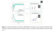
An Adjustment Strategy for Tilted Moiré Fringes via Deep Q-Network​


National Key Laboratory of Optical Field Manipulation Science and Technology
State Key Lab of Optical Technologies on Nano-Fabrication and Micro-Engineering
Institute of Optics and Electronics, Chinese Academy of Sciences
University of Chinese Academy of Sciences

Abstract​

Overlay accuracy, one of the three fundamental indicators of lithography, is directly influenced by alignment precision. During the alignment process based on the Moiré fringe method, a slight angular misalignment between the mask and wafer will cause the Moiré fringes to tilt, thereby affecting the alignment accuracy. This paper proposes a leveling strategy based on the DQN (Deep Q-Network) algorithm. This strategy involves using four consecutive frames of wafer tilt images as the input values for a convolutional neural network (CNN), which serves as the environment model. The environment model is divided into two groups: the horizontal plane tilt environment model and the vertical plane tilt environment model. After convolution through the CNN and training with the pooling operation, the Q-value consisting of n discrete actions is output. In the DQN algorithm, the main contributions of this paper lie in three points: the adaptive application of environmental model input, parameter optimization of the loss function, and the possibility of application in the actual environment to provide some ideas. The environment model input interface can be applied to different tilt models and more complex scenes. The optimization of the loss function can match the leveling of different tilt models. Considering the application of this strategy in actual scenarios, motion calibration and detection between the mask and the wafer provide some ideas. To verify the reliability of the algorithm, simulations were conducted to generate tilted Moiré fringes resulting from tilt angles of the wafer plate, and the phase of the tilted Moiré fringes was subsequently calculated. The angle of the wafer was automatically adjusted using the DQN algorithm, and then various angles were measured. Repeated measurements were also conducted at the same angle. The angle deviation accuracy of the horizontal plane tilt environment model reached 0.0011 degrees, and the accuracy of repeated measurements reached 0.00025 degrees. The angle deviation accuracy of the vertical plane tilt environment model reached 0.0043 degrees, and repeated measurements achieved a precision of 0.00027 degrees. Moreover, in practical applications, it also provides corresponding ideas to ensure the determination of the relative position between the mask and wafer and the detection of movement, offering the potential for its application in the industry.​


1721428478768.png

Please, Log in or Register to view URLs content!
 

gelgoog

Lieutenant General
Registered Member
@zeljo024
I doubt Tokyo Electron uses that many US components in their tools to begin with.
ASML is dependent on light sources from their US Cymer division however. So their tools won't work without US components.
 

siegecrossbow

General
Staff member
Super Moderator
Conspiracy theory that no one from both of the aisles have mentioned — is it possible that Chinese fabs/toolmakers are starting to proactively lobby (via second or third party) for additional bans/sanctions by the U.S. Congress to squeeze out foreign competition?
 

huemens

Junior Member
Registered Member
Conspiracy theory that no one from both of the aisles have mentioned — is it possible that Chinese fabs/toolmakers are starting to proactively lobby (via second or third party) for additional bans/sanctions by the U.S. Congress to squeeze out foreign competition?
No need for that. The US has to continuously do something like this for political benefit, especially with the election coming up. Note that there are announcements like this every few weeks and many of those are just for headlines with little to no practical change in the existing situation.
 
Top