Chinese semiconductor thread II

tokenanalyst

Brigadier
Registered Member

Oriental Jingyuan YieldBook 3.0 "BUFF Stacked" DMS+YMS+MMS three major systems enable integrated circuit yield management​


Yield is an important indicator in chip manufacturing. If the advanced process represents the leading edge of wafer fab technology, then the product yield represents the reliability and economy of its products. Under the condition of fixed manufacturing cost, the higher the yield, the lower the cost of a single chip. Every step in wafer design and manufacturing affects the yield of the chip. Therefore, the key to improving chip yield lies in complete and effective monitoring and testing of the manufacturing process, while analyzing the data in the manufacturing process to promptly identify problems and potential risks, and feedback to the integrated circuit manufacturing and design ends to improve the process and design.
1721225898038.png
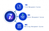
Aiming at this demand and pain point of the industry, Oriental Crystal Source launched the yield management platform YieldBook. After more than two years of iterative upgrades, version 3.0 was recently launched. This version gives full play to Oriental Crystal Source's advantages in computational lithography software OPC and electron beam measurement and testing equipment, becoming the industry's first one-stop yield management software to achieve comprehensive measurement data (MMS), defect data (DMS), and yield data (YMS). It can perform individual process quality monitoring, overall defect rate statistics, yield loss traceability analysis, feedback manufacturing difficulties to the upstream design end, etc., comprehensively monitor factors affecting yield and assist in yield improvement.
Three major systems cover all data types of Fab to achieve one-stop yield management throughout the entire process
The factors affecting the yield of chip products may include design, process and equipment. A complete root cause analysis of the yield requires a comprehensive analysis of data from these three aspects, so the ability of yield management depends on the size of the data range analyzed. In the past, FAB engineers needed to use a variety of tools such as MMS, DMS, and YMS. The YieldBook yield management platform brings together the three major systems of MMS, DMS, and YMS, which can realize the analysis of all data types of Fab. It is worth mentioning that the YieldBook platform is not a simple carrier for the above three systems. It can realize cross-analysis of underlying data between different systems, providing more benefits for yield management.
Four major features "support" yield management adds "new gameplay"
The YieldBook yield management platform also has four major features that bring "new ways of playing" to FAB engineers. (1) Defect Similar Pattern Map Search: Select the base wafer in the Map gallery, set the search conditions in multiple dimensions, and automatically present the search similar results for engineers to further analyze and find the cause of the defect; (2) PME (Process Margin Explorer): Based on the D2DB defect detection algorithm, the wafer inspection image is compared with the design layout to identify the defect layout information that affects the process window; (3) Auto Ink: Supports automatic/manual calibration of the entire area or partical area of a single or batch wafer, improving the efficiency of Inkless Map calibration when the wafer is shipped; (4) RDMS (Reticle Defect Management System): Analyze Retical related data, and present the analysis results in the form of defect heat map, repeated defect number summary, scan defect data chart, etc., so as to achieve defect management of the mask.

Please, Log in or Register to view URLs content!
 

tokenanalyst

Brigadier
Registered Member

UPH up to 120K, the world's first "mass transfer FOPLP" advanced packaging line goes into mass production.​


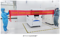
Recently, Plasmo's P-XBonder mass transfer panel-level wafer piercing machine passed customer acceptance, marking the mass production of the world's first "mass transfer FOPLP" advanced packaging line.
1721226168296.png

With TSMC, Samsung and other companies deploying panel-level packaging (PLP) related technologies, including fan-out panel-level packaging (Fan-Out -PLP, referred to as FO-PLP), FOPLP has become an industry hotspot. Compared with wafer-level packaging, the larger the substrate size of panel-level packaging, the larger the size of the corresponding equipment, the longer the path of the Pick & Place action, and the higher requirements for the accuracy, efficiency, consistency and stability of the motion mechanism of the equipment.

For panel-level packaging, Plexicon has creatively developed the mass transfer panel-level die bonding machine P-XBonder, which adopts the flip-chip die bonding method to realize the mass transfer of Die from Wafer to substrate. The production capacity per hour (UPH) reaches 120K, the mounting accuracy is ±15μm@3σ, and the highest mounting accuracy reaches ±5μm@3σ. It is suitable for panel-level packaging of substrates such as metal panels, glass panels, and printed circuit boards, and can be applied to both chip first and chip last board-level packaging processes.​

Please, Log in or Register to view URLs content!
 

tokenanalyst

Brigadier
Registered Member

Fadong EDA electromagnetic brain innovates China's local FDSPICE®​


The rapid development and widespread application of 5G and 5.5G have brought new challenges and higher requirements to the original analog circuit simulation tools. The market and users require circuit simulation tools to have higher accuracy, stronger computing power and more flexible functions to support 5G and 5.5G analog/RF circuit system simulation and optimization.

In order to respond to and adapt to this challenge and user needs, China's leading RF EDA brand, Fadong EDA, has successfully developed the system-level circuit simulation design platform FDSPICE ® .

FDSPICE ® is mainly used for system-level circuit simulation and parameter optimization of large-scale analog/RF, microwave/millimeter wave, and high-speed digital circuits. FDSPICE ® uses advanced AI technology and the patented "FadEDA Electromagnetic Brain" technology (patent announcement number "CN 108182316B") to quickly simulate and optimize the circuit schematics and layouts.

Please, Log in or Register to view URLs content!
 

Hyper

Junior Member
Registered Member
Bloomberg video says that insiders say they will not comply with initial sanctions (the first few rounds they are complying with) if restrictions are increased. I think Cymer will start production with Trumpf.
 

tokenanalyst

Brigadier
Registered Member

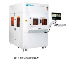
Youruipu successfully delivered SICD200 equipment to overseas customers​


Recently, Shanghai Unipu Semiconductor Equipment Co., Ltd. ("Uripu") successfully delivered to an overseas customer a fully automatic equipment for dislocation and micropipe detection of silicon carbide substrate wafers.

Dr. Tang Deming, General Manager of Youruipu, introduced the following technical features of SICD200 :

  • Compatible with 6&8 inch SiC substrate dislocation and micropipe defect detection; the equipment is fully automatic;
  • High-resolution real-time focusing high-speed line scanning imaging technology increases the detection rate by more than ten times compared with traditional area scanning, and realizes full detection of dislocation defects of the entire wafer (corrosion wafer), which greatly reduces the number of equipment purchased by customers;
  • Adopt deep learning algorithm (AI) to effectively improve the accuracy of dislocation detection and realize dislocation classification;
  • Can be connected to the MES system of silicon carbide substrate manufacturers, realize factory automation production;
  • The equipment provides a crystal internal stress detection function, which can be used for silicon carbide seed crystal screening.

1721233639507.png


Please, Log in or Register to view URLs content!
 

tokenanalyst

Brigadier
Registered Member

Illumination Field Uniformity Correction by Novel Finger Arrays for Lithography Illumination System​


School of Optical and Electronic Information, Huazhong University of Science and Technology,
Institute of Optics and Electronics, Chinese Academy of Sciences
University of Chinese Academy of Sciences

Abstract​

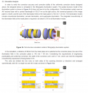
In order to correct the integrated nonuniformity of a lithographic illumination field, a high-precision uniformity correction method for an advanced lithographic illumination system is proposed. The method adopts the opaque finger array structure and improves correction ability and accuracy by optimizing the arrangement and structure of the unit without changing the width of each unit. The correction accuracy is expressed as the percentage of the corrected integrated nonuniformity. Through theoretical analysis and simulation, it can be seen that the correction accuracy of a staggered finger array is better than 0.22%. When staggered and layered, the correction accuracy of a finger array is better than 0.14%, which is better than that of a non-layered finger array. When staggered, layered, and chamfered of each unit, the correction accuracy of the finger array structure is better than 0.12%.​


1721235939958.png
Please, Log in or Register to view URLs content!
 

gelgoog

Brigadier
Registered Member
What is the impact of Chinese semiconductor chip production?

bloomberg

US Floats Tougher Trade Curbs in Chip Crackdown on China​

  • Restrictions would hit technology from Tokyo Electron and ASML
ASML said in a statement that second-quarter net sales were 6.24 billion euros, exceeding market expectations of 6 billion euros. Bookings increased 54% to 5.57 billion euros ($6.1 billion), exceeding the consensus of 4.41 billion euros.
China accounted for almost half of ASML's second quarter sales, up €390 million from the previous quarter.
They could delay the current Chinese fab expansion. Maybe it would get stuck halfway. Instead of a capacity increase of like half a million wafers per month you would get half that. But in the long term it would actually help China since all those tool orders would go to Chinese vendors instead.
 

GiantPanda

Junior Member
Registered Member
They could delay the current Chinese fab expansion. Maybe it would get stuck halfway. Instead of a capacity increase of like half a million wafers per month you would get half that. But in the long term it would actually help China since all those tool orders would go to Chinese vendors instead.

I imagine that China's firms are buying from the West as long as goods are still available. But they are not buying these things as part of long term contracts experting deliveries far into the future. At least, they shouldn't. Any Chinese company that still plans their growth around Western tech exclusively deserves what's coming to them when the ban happens.

But nothing wrong with stocking up when they are still available and China has shown over the last two years, they have no trouble servicing them locally. To stop buying before the ban actually happens simply means you are extending the ban prematurely yourself.
 

gelgoog

Brigadier
Registered Member
One thing I noticed with the YMTC and CXMT production sites is that they changed the original schematics and plan for the fab expansions. They used to have a large single building, and they were supposed to add another one per expansion. But the thing is they went with two smaller buildings instead of a large one. So something clearly changed here.
 
Top