Chinese semiconductor thread II

tokenanalyst

Brigadier
Registered Member

Investigation of an electrode-driven hydrogen plasma method for in situ cleaning of tin-based contamination.​


1.Key Laboratory of Radiation Physics and Technology, Ministry of Education, Institute of Nuclear Science and Technology, Sichuan
2.Institute of Atomic and Molecular Physics, Sichuan University,
3.Institute of High Performance Scientific Computation, Xihua University,
4.School of Engineering Science, University of Chinese Academy of Sciences,

Abstract​

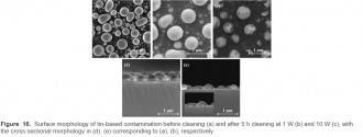
To prolong the service life of optics, the feasibility of in situ cleaning of the multilayer mirror (MLM) of tin and its oxidized contamination was investigated using hydrogen plasma at different power levels. Granular tin-based contamination consisting of micro- and macroparticles was deposited on silicon via physical vapor deposition (PVD). The electrode-driven hydrogen plasma at different power levels was systematically diagnosed using a Langmuir probe and a retarding field ion energy analyzer (RFEA). Moreover, the magnitude of the self-biasing voltage was measured at different power levels, and the peak ion energy was corrected for the difference between the RFEA measurements and the self-biasing voltage (RFEA−self). XPS analysis of O 1s and Sn 3d peaks demonstrated the chemical reduction process after 1 W cleaning. Analysis of surface and cross-section morphology revealed that holes emerged on the upper part of the macroparticles while its bottom remained smooth. Hills and folds appeared on the upper part of the microparticles, confirming the top-down cleaning mode with hydrogen plasma. This study provides an in situ electrode-driven hydrogen plasma etching process for tin-based contamination and will provide meaningful guidance for understanding the chemical mechanism of reduction and etching.​

1721162574742.png
1721162611561.png

Please, Log in or Register to view URLs content!
 

tokenanalyst

Brigadier
Registered Member

Gallium Semiconductor's wafer-level (010) gallium oxide single crystal substrate diameter exceeds 3 inches​


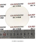
Hangzhou Gallium Semiconductor Co., Ltd. made a breakthrough in gallium oxide crystal growth and substrate processing technology, and successfully prepared a 3-inch wafer-level (010) gallium oxide single crystal substrate, which is the largest size reported internationally and has reached the international leading level.
1721162892856.png
Among the common mainstream crystal planes of gallium oxide single crystal substrates, (010) substrates have excellent performance in physical properties and epitaxy. First, (010) substrates have the highest thermal conductivity, which is conducive to improving the performance of power devices; second, (010) substrates have a faster epitaxial growth rate; third, devices prepared based on (010) substrates have better performance. At present, Gallium Semiconductor has launched wafer-level (010) gallium oxide single crystal substrate products, which are aimed at the scientific research market, meet the demand for (010) substrates in the scientific research field, and promote industry-university-research collaboration.

Hangzhou Gallen Semiconductor Co., Ltd. is mainly engaged in the research and development and production of semiconductor single crystal materials such as gallium oxide. It has been approved as a national-level science and technology-based small and medium-sized enterprise and an innovative small and medium-sized enterprise in Zhejiang Province. It has also taken the lead in obtaining approval for multiple projects such as the "Leading Goose" project of the Zhejiang Provincial Department of Science and Technology, and has strong production and R&D capabilities.

Please, Log in or Register to view URLs content!
 

measuredingabens

Junior Member
Registered Member

Please, Log in or Register to view URLs content!

Please, Log in or Register to view URLs content!

Flexible, permeable and 3D integrated electronic skin combines liquid metal circuits with fibrous substrates​


Please, Log in or Register to view URLs content!

Reliable 3D hybrid interfaces using ultrastretchable hLM solder. Credit: Zhuang et al.
In recent years, research teams worldwide have been trying to develop new flexible and soft electronics. These devices could have various potential applications, for instance helping doctors to monitor their patients' health conditions or supporting rehabilitation and performance sports.

To be safely and comfortably worn by users daily, these devices should be permeable (i.e., based on breathable materials that allow liquids and gases to pass through them). They should also be bio-compatible (i.e., safe to be worn on the human body for long periods of time) and strain resistant, meaning that they do not break easily when stretched or pulled in a specific direction.
Researchers at the Hong Kong Polytechnic University and other institutes in China recently developed a new intrinsically permeable, 3D integrated and flexible electronic skin. This e-skin, presented in a
Please, Log in or Register to view URLs content!
in Nature Electronics, is based on high-density inorganic electronic components placed on organic stretchable fibrous substrates.
"Most stretchable electronic systems have low-density integration and are wired with external printed
Please, Log in or Register to view URLs content!
, which limits functionality, deteriorates user experience and impedes long-term usability," Qiuna Zhuang, Kuanming Yao and their colleagues wrote in their paper. "We report an intrinsically permeable, three-dimensional integrated electronic skin."
Instead of utilizing impermeable and rigid printed circuit bords, Zhuang, Yao and their colleagues used a skin-like multilayered circuit board based on stretchable and permeable materials. This micropatterned circuit board is made of liquid metal and fiber mats.

"The system combines high-density inorganic electronic components with organic stretchable fibrous substrates using three-dimensional patterned, multilayered liquid metal circuits and stretchable hybrid liquid metal solder," the researchers wrote. "The electronic skin exhibits high softness, durability, fabric-like permeability to air and moisture and sufficient biocompatibility for on-skin attachment for a week."
The new stretchable material developed by the researchers was found to be highly resistant to strain, retaining its electrical properties up to an impressive strain of 1,500%. Moreover, the electronic skin can let both air and moisture pass through, preventing rashes and skin inflammation after being worn for long periods of time.
When they compared their proposed material to a previously developed stretchable electronic skin based on the material polydimethylsiloxane (PDMS), the team found that it was significantly thinner and less rigid. To further demonstrate its performance, the researchers used their electronic skin to develop bio-electronic devices that can record and wirelessly transmit physiological signals to another
Please, Log in or Register to view URLs content!
.
"We use the platform to create wireless, battery-powered and battery-free skin-attached bioelectronic systems that offer complex system-level functions, including the stable sensing of biosignals,
Please, Log in or Register to view URLs content!
and analysis, electrostimulation and
Please, Log in or Register to view URLs content!
," the research team wrote.
In the future, the inherently permeable and flexible
Please, Log in or Register to view URLs content!
developed by this team of researchers could be used to fabricate a wide range of devices for the reliable and safe monitoring of physiological processes. In addition, it could inspire the design of similar bio-compatible devices based on flexible circuit boards and
Please, Log in or Register to view URLs content!
solders.


gotodistance

New Member
Registered Member
What is the impact of Chinese semiconductor chip production?

bloomberg

US Floats Tougher Trade Curbs in Chip Crackdown on China​

  • Restrictions would hit technology from Tokyo Electron and ASML

ASML said in a statement that second-quarter net sales were 6.24 billion euros, exceeding market expectations of 6 billion euros. Bookings increased 54% to 5.57 billion euros ($6.1 billion), exceeding the consensus of 4.41 billion euros.
China accounted for almost half of ASML's second quarter sales, up €390 million from the previous quarter.
 

PopularScience

Junior Member
Registered Member
What is the impact of Chinese semiconductor chip production?

Please, Log in or Register to view URLs content!

US Floats Tougher Trade Curbs in Chip Crackdown on China​

  • Restrictions would hit technology from Tokyo Electron and ASML

ASML said in a statement that second-quarter net sales were 6.24 billion euros, exceeding market expectations of 6 billion euros. Bookings increased 54% to 5.57 billion euros ($6.1 billion), exceeding the consensus of 4.41 billion euros.
China accounted for almost half of ASML's second quarter sales, up €390 million from the previous quarter.

maybe ASML should stop selling to usa instead
 

ansy1968

Brigadier
Registered Member
What is the impact of Chinese semiconductor chip production?

bloomberg

US Floats Tougher Trade Curbs in Chip Crackdown on China​

  • Restrictions would hit technology from Tokyo Electron and ASML

ASML said in a statement that second-quarter net sales were 6.24 billion euros, exceeding market expectations of 6 billion euros. Bookings increased 54% to 5.57 billion euros ($6.1 billion), exceeding the consensus of 4.41 billion euros.
China accounted for almost half of ASML's second quarter sales, up €390 million from the previous quarter.
I eagerly await for it to happen, cause the moment they do implement it will force the Chinese gov't to officially unveil the mass production and mass usage of SSA800A and the introduction of SSA900A just to spite the American. It foreshadow what we predicted will happened on Oct 1 the 75th anniversary of the PROC and the American doesn't disappoint. ;)
 

mst

Junior Member
Registered Member
The moves came after
Please, Log in or Register to view URLs content!
on Wednesday reported that the Biden administration is considering a wide-sweeping rule to clamp down on companies exporting their critical chipmaking equipment to China.

Washington’s foreign direct product rule, or FDPR, allows the U.S. to put controls on foreign-made products even if they use the smallest amount of American technology. This can affect non-U.S. companies.
 

tokenanalyst

Brigadier
Registered Member
The moves came after
Please, Log in or Register to view URLs content!
on Wednesday reported that the Biden administration is considering a wide-sweeping rule to clamp down on companies exporting their critical chipmaking equipment to China.

Washington’s foreign direct product rule, or FDPR, allows the U.S. to put controls on foreign-made products even if they use the smallest amount of American technology. This can affect non-U.S. companies.
I doubt that they could implement this without causing anger given that HALF of US tools companies revenue comes from China. Much more than European companies or most Japanese companies.
Maybe the Europeans should implement their own FDPR so when US companies sell technology to someone the EU doesn't like they could sanction US companies too. Or even better I know that ASML use some Chinese components and materials in their machines, maybe China should apply their FDPR to ASML and say you shouldn't ship these tools to the US or even give them service.
 
Top