Chinese semiconductor thread II

tokenanalyst

Brigadier
Registered Member

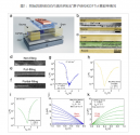
Zhang Zhiyong's research group at the School of Electronics has realized low-power tunneling transistors based on perovskite-doped carbon nanotubes​


Silicon-based complementary metal oxide semiconductor (CMOS) technology has entered the 5-nanometer technology node in 2022, and the characteristic size of transistors is close to the physical limit. Seeking new materials and new principles of semiconductor integrated circuit technology has become the focus of attention in academia and industry. Carbon nanotubes (CNTs) have excellent electrical properties, quasi-one-dimensional lattice structure, high carrier mobility and other characteristics. They are one of the ideal semiconductor channel materials for building new CMOS transistors and integrated circuits. Unlike traditional silicon-based semiconductor materials, carbon nanotubes are composed of CC sp 2 covalent bonds, have strong chemical stability, and are difficult to achieve controllable and stable doping, which greatly limits the electrical control freedom of carbon-based devices.
1720719190869.png

Recently, the research groups of Professor Zhang Zhiyong from the Carbon-based Electronics Research Center of the School of Electronics, Peking University, and the Laboratory of Physics and Chemistry of Nanodevices of the Ministry of Education, Professor Jin Chuanhong from Zhejiang University, and Researcher Zhu Maguang from Nanjing University have successfully filled one-dimensional perovskite materials (CsPbBr 3 /CsSnI 3 ) into carbon nanotubes using the gas phase/liquid phase self-assembly filling technology of carbon nanotubes, regulated the electrical properties, and successfully constructed internally doped carbon nanotube CMOS transistors. More importantly, the team designed and demonstrated for the first time a broken-gap tunneling transistor (TFET) based on a half-filled perovskite-carbon nanotube (CsPbBr 3 /CNT) coaxial heterojunction. The room temperature subthreshold swing of the device is about 35 mV dec -1 , and the on-off current ratio is greater than 10 5 , demonstrating the application prospects of one-dimensional perovskite-doped carbon nanotube materials in the construction of high-performance and ultra-low power integrated circuits.

Please, Log in or Register to view URLs content!
 

GiantPanda

Junior Member
Registered Member
The Chinese EDA industry is rapidly improving the capabilities of their software. I think without the US sanctions on sales of EDA software it wouldn't have happened.

That statement is an absolute certainty. China is cut-throat capitalistic. If Chinese companies could buy from established companies like Cadence or Synopsys they would do it -- because frankly it would be far less risky than buying from a local firm with far less customers.

The sanctions flipped both the risk calculation and drove a new stream of customers to the domestic tools industry at the same. This created the virtuous feedback loop of domestic equiptment maker to products to customers to equiptment maker. Especially important in the semicon industry where feedback that improves a product over time needs to come from the production lines.

That virtuous feedback loop, even on Chinese soil, until the trade war was used mainly for foreign equipment makers not domestic ones. This is the real sea-change. Chinese EDA like Empyrean -- as well as all the other equipment makers -- will now improve and expand much faster than before because their products will be in the production lines and they will be given the opportunity now to iterate year after year to improve their products.
 

GiantPanda

Junior Member
Registered Member
Not going to disclose source so take it with a mountain of salt but there is a rumor that the PRC now has complete supply chain for producing high end semiconductor.

Depending on what is high end (sub 5mn?) -- this could mean either a domestic EUV or a domestic DUV used in a process (assumed to be multi-patterning) that can bring us to a high end node.
 

tokenanalyst

Brigadier
Registered Member
Not going to disclose source so take it with a mountain of salt but there is a rumor that the PRC now has complete supply chain for producing high end semiconductor.
I would say that right now they have a completely domestic wafer fabs. I know there is one in Shanghai were SMEE, NAURA and others equipment makers are using for their tools and there is another in a district in Beijing , Huawei is also making a fab but for "low" to "mid" end chips but probably not 100% domestic.
 

tokenanalyst

Brigadier
Registered Member

ACCOTEST launching new test tool for high end SOCs by end of this year, completed last year tools orders and expanding overseas.​


New tool.

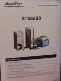
in June 2023, the company launched a new generation of models STS8600 for the first time. The test system has more test channels and higher test frequencies, which further improves the company's product line and broadens the testable range of the company's products, providing a strong boost to the company's future long-term development. As of March 2024, the STS8600 model has been able to cover the testing of large-scale SoC chips (high-speed digital circuits, high-performance hybrid circuits, microwave/RF circuits, communication interface circuits, CPU chips, etc.). So far, the company is developing new boards and conducting customer verification for this model. In the future, after the company launches STS8600 on the market, the test coverage of the company's products will more than double. As the company's product test coverage continues to expand and its product market share continues to increase, the company's future performance growth space is expected to be opened.
1720730870059.png

Orders

Revenue, the order volume for the whole of last year has been completed in the first half of this year." Sun Qi said that on the one hand, the company's tester products have expanded from traditional simulation to SoC, mixed analog and digital, and power, and are in an advantageous position among similar products in terms of product performance and market share; on the other hand, the company's main business belongs to the manufacture of special equipment for semiconductor materials, serving the main industrial links of the semiconductor industry from design to packaging and testing.

Overseas.

Huafeng Measurement & Control's core markets include the United States, Japan, and Malaysia. "Last year, the company implemented the construction of an overseas production center in Malaysia, and now Huafeng Measurement & Control's factory in Penang, Malaysia has been officially put into use."

"The overseas production center was located in Malaysia in response to the overseas business needs of downstream customers. For example, power semiconductor giant Infineon Technologies and Huatian Technology have set up operations in the region." A person from the secretary's office of Huafeng Measurement & Control said that as the market warms up and the economic climate continues to recover, overseas markets represented by Southeast Asia will also contribute orders one after another.

Please, Log in or Register to view URLs content!
 

Blitzo

Lieutenant General
Staff member
Super Moderator
Registered Member
Not going to disclose source so take it with a mountain of salt but there is a rumor that the PRC now has complete supply chain for producing high end semiconductor.


Depending on what is high end (sub 5mn?) -- this could mean either a domestic EUV or a domestic DUV used in a process (assumed to be multi-patterning) that can bring us to a high end node.

What is considered high end in this case. Is it the same as the sanction's target? 14nm?

Giantpanda and proelite are correct -- "high end" is rather vague. If the original rumour was also vague then that's fine, but that should be the natural first question or at least something to acknowledge.

Is it meeting the threshold of sub 14nm, or sub 7nm or even sub 5nm etc.


Of course, further domestic self sufficiency for the semiconductor production line is something that has been predicted for a long time, the real question is if there is some sort of milestone that's been claimed to have been attained, what actual milestone is it?

The question after that, is what would the speed of implementation and upscaling be
 
Top