I'm pretty sure this isn't going to be a real problem because of constraints from both sides. Chinese government is well aware and will insist on prioritizing domestic supply before exports. Further given the example of US government forcing Apple to abandon its previously contemplated partnership before it's quite plausible that the US government will shut this down as well so there might not be any exports anyway.I really hope that the government put limits on how many memory US companies can buy, so the domestic supply doesn't dry up. After all this is a problem of their own making. Letting US AI companies to buy unpatterned wafer supply to limit competition and delaying CXMT and YMTC capacity build up.

You are using an out of date browser. It may not display this or other websites correctly.
You should upgrade or use an alternative browser.
You should upgrade or use an alternative browser.
Chinese semiconductor thread II
- Thread starter vincent
- Start date
I really hope that the government put limits on how many memory US companies can buy, so the domestic supply doesn't dry up. After all this is a problem of their own making. Letting US AI companies to buy unpatterned wafer supply to limit competition and delaying CXMT and YMTC capacity build up.
According to SMIC CEO in the latest earnings call, memory for consumer electronics like smartphone or laptops isn't a big bottle neck. Fabs can get the equipment to scale up front-end in 4-12 months depending on priority. CXMT / YMTC should absolutely scale up and take as much Apple orders as they can.
The bottleneck is more for HBM which is harder to scale apparently and needs more extensive customer validation

My impression just 1 or 2 years ago was that CXMT was a really small player with many challenges and YMTC had more chance of making it in the NAND market than CXMT had in the DRAM market
And now with the DRAM shortage suddenly they're getting removed from bans and lots of manufacturers are considering using them
Things are changing so quickly nowadays
And now with the DRAM shortage suddenly they're getting removed from bans and lots of manufacturers are considering using them
Things are changing so quickly nowadays
Low-overhead protection cryptographic chips become a core highlight of ISSCC, marking a key step for Muchuang's "Chinese chips" towards practical application.
At ISSCC 2026, China's Muchuang Integrated Circuit Design Co., Ltd. achieved a major milestone by having its low-overhead provably secure SHA-3 cryptographic chip selected as one of only two highlight papers in the conference’s inaugural Hardware Security session crowning it a global benchmark for innovation. This breakthrough directly addresses the long-standing industry challenge of balancing high security with prohibitive cost and energy consumption, achieving just 17% area overhead and 27% energy overhead, a dramatic improvement over traditional provably secure designs that often require more than double the resources.
The chip’s architectural innovation lies in three key advances: an asymmetric masking mechanism that reduces register usage by intelligently partitioning internal data; glitch-free dual-track precharge logic to eliminate signal leaks and side-channel vulnerabilities at the hardware level; and a hybrid single/dual-track architecture that applies high-security design only where essential, optimizing performance and efficiency without compromising security. These innovations collectively deliver provable security with zero latency increase making high-level protection viable even for low-power IoT devices and edge terminals.
This achievement is part of Muchuang’s sustained trajectory of leadership in cryptographic hardware. Over recent years, the company has consistently presented groundbreaking research at ISSCC (2022–2026), including the world's first post-quantum chip supporting multiple NIST-standardized algorithms, a transferable quantum-resistant chip developed with Tsinghua University, and an energy-efficient fully homomorphic encryption processor capable of secure computation across cloud and edge environments all demonstrating its systemic R&D strength and commitment to foundational security technologies.
Beyond technical excellence, Muchuang’s work is driving national progress in information security. With over 40 million network chips shipped, the company is enabling secure infrastructure for AI, cloud computing, and next-generation networks while breaking foreign technological monopolies. Its innovations are accelerating China’s march toward independent control of high-end cryptographic chips and laying a robust foundation for digital sovereignty, setting a new global standard in hardware security and positioning Chinese semiconductor technology at the forefront of the future information age.
Focusing on the R&D and industrialization of MEMS probe cards, MyMos Probe Cards has secured Series B+ funding.
MEMS Probe Card completed its Series B+ financing round, invested by Dark Shell Investment (Shenzhen) Co., Ltd., a subsidiary of Matrix Partners. MEMS Probe Card focuses on key links in the semiconductor industry chain, specializing in the R&D and industrialization of MEMS probe cards and electronic-specific materials. This round of financing will be used to accelerate breakthroughs in core technologies, expand production lines, and attract high-end talent.

Biren Technology's patents for "tensor core, processor, data processing method, electronic device and storage medium" have been authorized.
According to Tianyancha, Shanghai Biren Technology Co., Ltd. recently obtained a patent entitled "Tensor Core, Processor, Data Processing Method, Electronic Device and Storage Medium", with authorization announcement number CN120803396B, authorization announcement date of December 9, 2025, and application date of September 12, 2025.
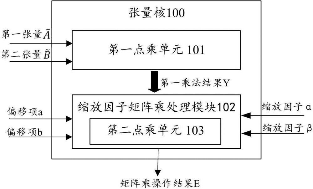
A tensor kernel, processor, data processing method, electronic device, and storage medium are disclosed, applicable to the field of tensor processing. The tensor kernel includes a first dot product unit and a scaling factor matrix multiplication processing module. The scaling factor matrix multiplication processing module includes a second dot product unit. The first and second dot product units support dot product operations with different floating-point precisions. The tensor kernel is configured to receive a first tensor, a second tensor, a scaling factor of the first tensor, a scaling factor of the second tensor, an offset term of the first tensor, and an offset term of the second tensor. The first dot product unit and the scaling factor matrix multiplication processing module are used to perform matrix multiplication operations using the scaling factor and the offset term, yielding the matrix multiplication result of the first and second tensors. By reusing dot product units of different precisions in the tensor kernel to perform matrix multiplication operations using scaling factors, the additional hardware area cost is reduced, and existing hardware resources are fully utilized.
Matched Threshold Voltage of n-Si/p-SiGe Hybrid-Channel Gate-All-Around CMOS Transistors Using a Single LaFMD Dipole with the Same n-Type Metal Gate
Abstract:
In this work, to address the issues of current mismatch and threshold voltage (VT) asymmetry in n/p GAAFETs, a single La(iPr2-FMD)3 (LaFMD) dipole combined with the same n-type metal gate (MG) is proposed for n-Si/p-SiGe hybrid-channel (HC) gate-all-around (GAA) CMOS transistor. First, after the same n-type MG is employed for this HC GAA CMOS transistor, a matched n/p drive current (ION) is achieved at same overdrive voltage |VGS| -|VT| = 0.6 V, but their VTN and VTP both exhibit positive shifts. Then, 5-cycle LaFMD dipole is further introduced to simultaneously obtain matched VT and ION. For example, matched VT of -0.25/0.28 V for pFET/nFET is attained. Meanwhile, this dipole can further improve the interface quality of the channel, resulting in lower SS (nFET: 75.5 to 66.0 mV/dec, pFET: 87.7 to 79.3 mV/dec). Owing to the matched VT, the inverter of this HC-GAAFET demonstrates good symmetry with a relatively high peak voltage gain of 35.26 V/V, further demonstrating its application potential.
First Demonstration of Deeply Scaled 2T0C DRAM With Record Data Retention and Fast Write Speed
Abstract:
In this work, the first pitch scaling of 2T0C dynamic random-access memory (DRAM) based on indium-tin-oxide (ITO) transistors has been successfully fabricated, achieving a record-low contact length of 20 nm and channel length of 10 nm. The deeply scaled 2T0C DRAM demonstrates multi-level operation with an ultra-fast write speed of 10 ns, facilitated by a high on-state current. Furthermore, it features an outstanding data retention time exceeding 3000 s, attributed to its low off-state leakage current of 1.3×10⁻²⁰ A/ μ m. This work highlights the tremendous potential of oxide semiconductor-based 2T0C DRAM for future high-density memory applications.
This definitely won't happen.I really hope that the government put limits on how many memory US companies can buy, so the domestic supply doesn't dry up. After all this is a problem of their own making. Letting US AI companies to buy unpatterned wafer supply to limit competition and delaying CXMT and YMTC capacity build up.
The US has tried to strangle China's chip industry by not allowing to buy advanced stuff for years. No way companies like CXMT would strangle themselves by selling their best stuff to the US after everything that's happened in the last few years.
It's always good to see that companies like CXMT and YMTC are gaining traction
The team led by Wang Xingjun and Shu Haowen at Peking University has achieved a new breakthrough in integrating photonics to enable fiber/wireless communication (6G).
On February 18, 2026, the research paper "Integrated photonics enabling ultra-wideband fibre–wireless communication" was published online in the top international academic journal *Nature*. The research team of Professor Wang Xingjun and Researcher Shu Haowen from the School of Electronic Engineering at Peking University, in collaboration with Academician Yu Shaohua's team from Pengcheng Laboratory, Associate Professor Chen Baile's team from ShanghaiTech University, and General Manager Xiao Xi's team from the National Information Optoelectronics Innovation Center, achieved a breakthrough in the fields of next-generation wireless communication (6G) and optical communication. They proposed the concept of integrated "fiber-wireless converged communication" for the first time internationally, and pioneered the seamless cross-network integration of fiber optic and wireless communication systems. Through a self-developed ultra-wideband optoelectronic converged integrated chip and AI-enabled advanced equalization algorithms, the system developed by this research institute can support world-record data transmission rates in all major telecommunications scenarios (including fiber optic, wireless, and hybrid links), achieving "one system, cross-scenario reuse."

