Chinese semiconductor thread II

gelgoog

Lieutenant General
Registered Member
This is pretty impressive. It basically has the same performance as the original AMD Zen processor. You could hardly expect much more. Since they are basically using a 14nm FinFET process from what I understand. So comparing it with 7nm or 5nm processors like he's also doing is a bit much. My guess is Loongson went for a quad core initially because they were expecting low yields. It only seems to have a couple weaknesses. The SMT performance boost could be better, and the floating point vector multiplication seems to be slower. It also has half the floating point fused multiply add vector units.
 

pevade

Junior Member
Registered Member
Moore Thread Intelligent Technology (Beijing) Co., Ltd. "Circuits and methods, chips, and computing equipment for data standardization" was published. The application publication date is March 12, 2024, and the application publication number is CN117692008A.

The present disclosure relates to a circuit for data normalization, including: an input terminal configured to receive initial data; a shift control circuit including an n-level detection circuit, wherein the i-th level detection circuit is configured to: respond to the initial data The first non-zero value of is not within the shift range of the i-level shift, and the first signal value is output, otherwise, the second signal value is output; the shift circuit includes an n-level sub-shift circuit, wherein the n-th sub-shift circuit The input data of the circuit is initial data, and the input data of other-level sub-shift circuits is the output data of the previous-level sub-shift circuit, in which the i-th sub-shift circuit is configured to: respond to the input signal from the i-th level detection circuit. The first signal value performs an i-level shift on the input data in the direction of the first bit and outputs the shifted data, or outputs the input data in response to the second signal value from the i-th level detection circuit; the output terminal is configured is: output the output data of the first-stage sub-shift circuit as normalized data.

View attachment 126668
Can anyone even explain WTF is this even supposed to be for? Because I've read the description several times and still coming up blank.
 

mst

Junior Member
Registered Member
Please, Log in or Register to view URLs content!

Bloomberg) -- The Chinese government has quietly asked electric-vehicle makers from BYD Co. to Geely Automobile Holdings Ltd. to sharply increase their purchases from local auto chipmakers, part of a campaign to reduce reliance on Western imports and boost China’s domestic semiconductor industry. The country’s tech overseer previously set an informal target for automakers to source a fifth their chips locally by 2025, but has grown dissatisfied with the pace of progress, the people said.

The ministry is now directly instructing firms to avoid foreign semiconductors if at all possible, said the people, who asked to remain anonymous discussing sensitive information. That means overseas chip firms effectively have to manufacture their silicon through a local foundry such as Semiconductor Manufacturing International Corp. or Hua Hong Semiconductor Ltd., one of the people said. During a recent tender conducted by a major domestic brand, one foreign bidder failed to secure a contract despite offering a price they estimated was 30% lower than the eventual winner, another person said.

The developments reflect Beijing’s stepped-up efforts to galvanize its own tech sector, a response to US attempts to curtail Chinese chip development via sanctions and restrictions on the sale of advanced technology. The Chinese directive on cars casts uncertainty over the business of companies from Nvidia Corp. and NXP Semiconductor NV to Renesas Electronics Corp. and Texas Instruments Inc., which compete with local firms to supply the world’s largest EV market.

Many local brands buy a hodge-podge of other components from power management chips to microcontrollers and display ICs. Some carmakers from leader BYD to upstarts like Nio Inc. rely on Nvidia processors for instance to coordinate functions in their hyper-connected cars.

Beijing is increasingly intent on supporting a domestic chip industry it knows is lagging well behind foreign rivals, but critical to supporting the economy and maintaining a geopolitical advantage. The directive is in line with pledges this year to mobilize all means at its disposal to wrest technological supremacy from the US and other nations.

The central government may also be bracing for curbs in the auto sector specifically.

Washington is probing potential data and cyber-security risks posed by internet-connected cars from China, including EVs. US Commerce Secretary Gina Raimondo has expressed concern that data collected by the cars could wind up in Beijing’s hands, and is overseeing an investigation that could result in restrictions on the sale of those cars in the US — measures that would go beyond a potential increase in tariffs.

A mandate in favor of Chinese chips also raises the prospect of further retaliation as Washington ramps up its containment campaign.

At the Two Sessions meeting of lawmakers this month, Beijing hammered home a longstanding goal to break an American stranglehold on key spheres. Under Xi Jinping’s watch, China has expanded state control of strategically critical areas from semiconductor manufacturing to quantum computing.

Against that backdrop, Beijing has endorsed the efforts of local champions such as Huawei Technologies Co. through subsidies and targeted policies. It’s now establishing a $27 billion-plus fund to drive chip investments and hiking spending on nationwide research to more than $51 billion.

China’s biggest auto chip and software providers include Huawei, Loongson Technology Corp., GigaDevice Semiconductor Inc. and Wingtech Technology Co. Many, like Novosense Microelectronics Co. and StarPower Semiconductor Ltd., have built significant capacity in so-called mature or lower-end nodes. The MIIT’s policy may soak up some of that capacity — at the expense of their foreign rivals.

The US and its European allies, meanwhile, have grown alarmed by China’s rush into older-generation chips. The Biden administration is mulling tariffs on those components in addition to other trade tools, but has said it is not considering restricting them using export controls.

While US rules introduced in 2022 slowed China’s development of advanced chipmaking capabilities, they left largely untouched the country’s ability to use techniques older than 14-nanometers. That has led Chinese firms to construct new plants faster than anywhere else in the world. They are forecast to build 26 fabs through 2026 that use 200-millimeter and 300-mm wafers, according to data from the trade group SEMI as of 2023. That compares with 16 fabs for the Americas.
 

tphuang

Lieutenant General
Staff member
Super Moderator
VIP Professional
Registered Member
Please, Log in or Register to view URLs content!

Bloomberg) -- The Chinese government has quietly asked electric-vehicle makers from BYD Co. to Geely Automobile Holdings Ltd. to sharply increase their purchases from local auto chipmakers, part of a campaign to reduce reliance on Western imports and boost China’s domestic semiconductor industry. The country’s tech overseer previously set an informal target for automakers to source a fifth their chips locally by 2025, but has grown dissatisfied with the pace of progress, the people said.

The ministry is now directly instructing firms to avoid foreign semiconductors if at all possible, said the people, who asked to remain anonymous discussing sensitive information. That means overseas chip firms effectively have to manufacture their silicon through a local foundry such as Semiconductor Manufacturing International Corp. or Hua Hong Semiconductor Ltd., one of the people said. During a recent tender conducted by a major domestic brand, one foreign bidder failed to secure a contract despite offering a price they estimated was 30% lower than the eventual winner, another person said.

The developments reflect Beijing’s stepped-up efforts to galvanize its own tech sector, a response to US attempts to curtail Chinese chip development via sanctions and restrictions on the sale of advanced technology. The Chinese directive on cars casts uncertainty over the business of companies from Nvidia Corp. and NXP Semiconductor NV to Renesas Electronics Corp. and Texas Instruments Inc., which compete with local firms to supply the world’s largest EV market.

Many local brands buy a hodge-podge of other components from power management chips to microcontrollers and display ICs. Some carmakers from leader BYD to upstarts like Nio Inc. rely on Nvidia processors for instance to coordinate functions in their hyper-connected cars.

Beijing is increasingly intent on supporting a domestic chip industry it knows is lagging well behind foreign rivals, but critical to supporting the economy and maintaining a geopolitical advantage. The directive is in line with pledges this year to mobilize all means at its disposal to wrest technological supremacy from the US and other nations.

The central government may also be bracing for curbs in the auto sector specifically.

Washington is probing potential data and cyber-security risks posed by internet-connected cars from China, including EVs. US Commerce Secretary Gina Raimondo has expressed concern that data collected by the cars could wind up in Beijing’s hands, and is overseeing an investigation that could result in restrictions on the sale of those cars in the US — measures that would go beyond a potential increase in tariffs.

A mandate in favor of Chinese chips also raises the prospect of further retaliation as Washington ramps up its containment campaign.

At the Two Sessions meeting of lawmakers this month, Beijing hammered home a longstanding goal to break an American stranglehold on key spheres. Under Xi Jinping’s watch, China has expanded state control of strategically critical areas from semiconductor manufacturing to quantum computing.

Against that backdrop, Beijing has endorsed the efforts of local champions such as Huawei Technologies Co. through subsidies and targeted policies. It’s now establishing a $27 billion-plus fund to drive chip investments and hiking spending on nationwide research to more than $51 billion.

China’s biggest auto chip and software providers include Huawei, Loongson Technology Corp., GigaDevice Semiconductor Inc. and Wingtech Technology Co. Many, like Novosense Microelectronics Co. and StarPower Semiconductor Ltd., have built significant capacity in so-called mature or lower-end nodes. The MIIT’s policy may soak up some of that capacity — at the expense of their foreign rivals.

The US and its European allies, meanwhile, have grown alarmed by China’s rush into older-generation chips. The Biden administration is mulling tariffs on those components in addition to other trade tools, but has said it is not considering restricting them using export controls.

While US rules introduced in 2022 slowed China’s development of advanced chipmaking capabilities, they left largely untouched the country’s ability to use techniques older than 14-nanometers. That has led Chinese firms to construct new plants faster than anywhere else in the world. They are forecast to build 26 fabs through 2026 that use 200-millimeter and 300-mm wafers, according to data from the trade group SEMI as of 2023. That compares with 16 fabs for the Americas.
These Bloomberg articles are waste of time. They don’t know the basics of China ev industry supply chain. It’s embarrassing to read this crap.
 

tokenanalyst

Brigadier
Registered Member

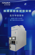
Technological innovation achieves new breakthroughs, North Huachuang releases a variety of 12-inch vertical furnace atomic layer deposition (ALD) equipment.​


Extremely large-scale advanced integrated circuit manufacturing technology continues to evolve, and the industry's requirements for related thin film growth equipment are increasing in terms of uniformity, step coverage, and thermal budget. Atomic layer deposition technology is widely recognized in the industry for its excellent shape retention, high step coverage and film thickness uniformity, but at the same time, its disadvantages of low deposition efficiency also need to be solved urgently. The batch processing characteristics of vertical furnaces make up for this shortcoming well, establishing the indispensable position of vertical furnace atomic layer deposition equipment in extremely large-scale advanced integrated circuit manufacturing.
1710515926440.png

In addition, vertical furnace atomic layer deposition equipment can also be equipped with a radio frequency plasma system to reduce the process temperature of thin film deposition and meet the needs of advanced processes for low thermal budget devices. Therefore, vertical furnace atomic layer deposition equipment has received widespread attention from the industry in recent years. It is widely used in storage, logic foundry and other fields of extremely large-scale advanced integrated circuit manufacturing. The domestic market size is expected to be approximately US$1 billion in the next three years.

Northern Huachuang closely follows the pace of industrial development and relies on its profound accumulation of vertical furnace equipment technology to develop and launch three 12-inch vertical furnace atomic layer deposition equipment, which have entered client verification and achieved large-scale mass production.

Plasma enhanced silicon nitride (PEALD Si 3 N 4 ) atomic layer deposition vertical furnace (product model: DEMAX SN302P) has made breakthroughs in radio frequency plasma generation and system control, in-situ cleaning, chamber flow field design, and furnace temperature A series of key technologies such as control and electrical software interactive fast response control. The equipment is widely used in extremely large-scale advanced integrated circuit storage and logic process device barrier layers (ALD Si 3 N 4 /HRP), sidewall insulation layers and doped thin film deposition (SiCN, SiBN) processes, and has won a number of logic and storage Orders from leading customers in the field, installed capacity and repeat orders have increased rapidly. As one of the first domestically produced plasma-enhanced silicon nitride atomic layer deposition vertical furnaces to be mass-produced, it provides reliable equipment support for extremely large-scale advanced integrated circuit manufacturing.

Low dielectric constant (Low-K) atomic layer deposition vertical furnace (product model: DEMAX CON302X) breaks through new technologies such as liquid source supply control, exhaust rapid switching control, in-situ cleaning and multi-element process control, reducing costs Dielectric constant of silicon source film. The equipment is mainly used in the gate sidewall film deposition process of 12-inch extremely large-scale integrated circuits to obtain a low dielectric constant and improve the corrosion resistance of the film. The process indicators are superior to similar products and meet the needs of large-scale integrated circuits for high-performance insulating layers. According to the demand, the equipment has now entered the client process verification stage.

The gap-filled silicon oxide atomic layer deposition vertical furnace (product model: DEMAX SN302T) breaks through the device high aspect ratio film filling and high-quality free radical oxide film deposition technology, optimizes the chamber flow field and air inlet pipe design, and significantly improves The film formation uniformity between wafers is improved, and good film insulation performance and device high aspect ratio filling effect are obtained. The equipment is mainly used in the silicon oxide insulating layer and dielectric filling layer in the storage field, and is especially widely used in the advanced technology node of 3D-NAND (flash memory) - the silicon oxide filling process of the insulating dielectric gap. In the memory array, the silicon oxide film plays a key role in the functions of the related front and rear film layers. It is the backbone equipment of the vertical furnace in the process of this field, and the market prospect is broad. Currently, the device is on the client side.

After years of technological innovation and industrialization verification, Northern Huachuang has achieved a comprehensive layout of vertical oxidation/annealing furnaces, vertical LPCVD and vertical ALD series equipment, and is expected to launch other vertical furnace atomic layer deposition equipment in the second half of this year. DEMAX series products.

Please, Log in or Register to view URLs content!
 

daifo

Major
Registered Member
A good watch on the Loongson 3600


The main point is that the cpu is "good enough." The primary problem for adoption outside of enterprise/gov is the software OS ecosystem. The options are:

1. Recompile and port of open source to loongson
2. Loongson optimized development and ports
3. Linux software running via x86/arm binary translation (50% in degrade performance)
4. Windows software running on WINE ontop of x86 translation (> 50% in degrade performance and stability)

The very popular and essential app WeChat is currently at 4. :) To transfer your wechat to a new phone, you currently need windows or a mac.

Simple Ports/Recompile sometime don't work as intended because it relies on specific instruction set or code specific to x86/arm to run. Sometime it is entire feature like rendering task and sometime it is simpler functions.
 
Last edited:

Wahid145

Junior Member
Registered Member

Technological innovation achieves new breakthroughs, North Huachuang releases a variety of 12-inch vertical furnace atomic layer deposition (ALD) equipment.​


Extremely large-scale advanced integrated circuit manufacturing technology continues to evolve, and the industry's requirements for related thin film growth equipment are increasing in terms of uniformity, step coverage, and thermal budget. Atomic layer deposition technology is widely recognized in the industry for its excellent shape retention, high step coverage and film thickness uniformity, but at the same time, its disadvantages of low deposition efficiency also need to be solved urgently. The batch processing characteristics of vertical furnaces make up for this shortcoming well, establishing the indispensable position of vertical furnace atomic layer deposition equipment in extremely large-scale advanced integrated circuit manufacturing.
View attachment 126699

In addition, vertical furnace atomic layer deposition equipment can also be equipped with a radio frequency plasma system to reduce the process temperature of thin film deposition and meet the needs of advanced processes for low thermal budget devices. Therefore, vertical furnace atomic layer deposition equipment has received widespread attention from the industry in recent years. It is widely used in storage, logic foundry and other fields of extremely large-scale advanced integrated circuit manufacturing. The domestic market size is expected to be approximately US$1 billion in the next three years.

Northern Huachuang closely follows the pace of industrial development and relies on its profound accumulation of vertical furnace equipment technology to develop and launch three 12-inch vertical furnace atomic layer deposition equipment, which have entered client verification and achieved large-scale mass production.

Plasma enhanced silicon nitride (PEALD Si 3 N 4 ) atomic layer deposition vertical furnace (product model: DEMAX SN302P) has made breakthroughs in radio frequency plasma generation and system control, in-situ cleaning, chamber flow field design, and furnace temperature A series of key technologies such as control and electrical software interactive fast response control. The equipment is widely used in extremely large-scale advanced integrated circuit storage and logic process device barrier layers (ALD Si 3 N 4 /HRP), sidewall insulation layers and doped thin film deposition (SiCN, SiBN) processes, and has won a number of logic and storage Orders from leading customers in the field, installed capacity and repeat orders have increased rapidly. As one of the first domestically produced plasma-enhanced silicon nitride atomic layer deposition vertical furnaces to be mass-produced, it provides reliable equipment support for extremely large-scale advanced integrated circuit manufacturing.

Low dielectric constant (Low-K) atomic layer deposition vertical furnace (product model: DEMAX CON302X) breaks through new technologies such as liquid source supply control, exhaust rapid switching control, in-situ cleaning and multi-element process control, reducing costs Dielectric constant of silicon source film. The equipment is mainly used in the gate sidewall film deposition process of 12-inch extremely large-scale integrated circuits to obtain a low dielectric constant and improve the corrosion resistance of the film. The process indicators are superior to similar products and meet the needs of large-scale integrated circuits for high-performance insulating layers. According to the demand, the equipment has now entered the client process verification stage.

The gap-filled silicon oxide atomic layer deposition vertical furnace (product model: DEMAX SN302T) breaks through the device high aspect ratio film filling and high-quality free radical oxide film deposition technology, optimizes the chamber flow field and air inlet pipe design, and significantly improves The film formation uniformity between wafers is improved, and good film insulation performance and device high aspect ratio filling effect are obtained. The equipment is mainly used in the silicon oxide insulating layer and dielectric filling layer in the storage field, and is especially widely used in the advanced technology node of 3D-NAND (flash memory) - the silicon oxide filling process of the insulating dielectric gap. In the memory array, the silicon oxide film plays a key role in the functions of the related front and rear film layers. It is the backbone equipment of the vertical furnace in the process of this field, and the market prospect is broad. Currently, the device is on the client side.

After years of technological innovation and industrialization verification, Northern Huachuang has achieved a comprehensive layout of vertical oxidation/annealing furnaces, vertical LPCVD and vertical ALD series equipment, and is expected to launch other vertical furnace atomic layer deposition equipment in the second half of this year. DEMAX series products.

Please, Log in or Register to view URLs content!
Always great to hear new Products by Naura, AMEC, Piotech among others. Can't fathom what's going to happen to AMAT, LAM, KLA & TEL in a couple of years
 
Top