Chinese semiconductor thread II

tphuang

Lieutenant General
Staff member
Super Moderator
VIP Professional
Registered Member
typical job advertising here by CETC
Please, Log in or Register to view URLs content!

Claims to be first in China to develop analog ICs. The only domestic firm to do CCD components and as good as any international players in SAW filters

Has full supply chain with 8-inch silcon IC production line, 4-inch InP opto IC line, 6 inch integrated special platform IC and more.
12 production lines in total. CETC is huge
 

measuredingabens

Junior Member
Registered Member
Please, Log in or Register to view URLs content!

Physical reservoir computing with emerging electronics

Abstract

Physical reservoir computing is a form of neuromorphic computing that harvests the dynamic properties of materials for high-efficiency computing. A wide range of physical systems can be used to implement this approach, including electronic, optical and mechanical devices. Electronics can, in particular, provide mixed-signal and fully analogue systems, and could be used to deliver large-scale implementations. Here we examine the development of physical reservoir computing with emerging electronics. We discuss the different architectures, physical nodes, and input and output layers of electrical reservoir computing. We also explore performance benchmarks and the competitiveness of different implementations. Finally, we consider the future development of the technology and highlight challenges that need to be addressed for it to deliver practical applications.
 

latenlazy

Brigadier
Is it a question of just shortage in relation to having domestic sources of capacity sufficient at present to replace suppliers

OR

Is it a question of not being able to produce the types of photoresists that are demanded in different nodes.

OR

Both

If it is the second, that's bad.

If it is the first, that can be easily resolved.
It’s not the second.
 

measuredingabens

Junior Member
Registered Member
Please, Log in or Register to view URLs content!

Pushing the thinness limit of silver films for flexible optoelectronic devices via ion-beam thinning-back process

Abstract

Reducing the silver film to 10 nm theoretically allows higher transparency but in practice leads to degraded transparency and electrical conductivity because the ultrathin film tends to be discontinuous. Herein, we developed a thinning-back process to address this dilemma, in which silver film is first deposited to a larger thickness with high continuity and then thinned back to a reduced thickness with an ultrasmooth surface, both implemented by a flood ion beam. Contributed by the shallow implantation of silver atoms into the substrate during deposition, the thinness of silver films down to 4.5 nm can be obtained, thinner than ever before. The atomic-level surface smooth permits excellent visible transparency, electrical conductivity, and the lowest haze among all existing transparent conductors. Moreover, the ultrathin silver film exhibits the unique robustness of mechanical flexibility. Therefore, the ion-beam thinning-back process presents a promising solution towards the excellent transparent conductor for flexible optoelectronic devices.
 

tphuang

Lieutenant General
Staff member
Super Moderator
VIP Professional
Registered Member
huawei/hisilicon unveils new Honghu media platform for smart home/entertainment systems.

Including T300/600/800/900 all with their own SoC & different support level

all have NearLink/wifi support for smart connection & communication between devices

Please, Log in or Register to view URLs content!
 

tokenanalyst

Brigadier
Registered Member

The first pan-semiconductor industry fund in Feixi, Anhui was established with a total scale of 500 million yuan.​


Feixi Industrial Investment news shows that Feixi’s first semiconductor industry fund was established. Recently, Hefei Precision Core Intelligent Venture Capital Fund Partnership (Limited Partnership) was registered in Feixi.

It is reported that the fund is managed by Accurate Capital as the fund manager, Hefei Accurate Xinqing Company as the general partner, Hefei High Quality Guidance Fund, Feixi Canal Fund of Funds, Shaoxing Lanyue Investment Company, Hainan Houdao Yiyi Fund, Accurate Huaxin Fund , Qingxinheng Fund, Hainan Yufeng Yian Fund, Huzhou Qiucheng Company, etc. were jointly established as limited partners. The total size of the fund is 500 million yuan, focusing on hard-core technology directions such as semiconductors. The main application scenarios revolve around industries such as new energy vehicles, robots and high-end manufacturing, metaverse and artificial intelligence.

Please, Log in or Register to view URLs content!
 

tokenanalyst

Brigadier
Registered Member

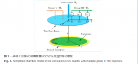
Optimization theory and application of epitaxial layer thickness uniformity in vertical MOCVD reaction chamber with multiple MO nozzles.​


Abstract​

Metal organic chemical vapor deposition (MOCVD) is a key means of epitaxy of heterojunction semiconductor material, the uniformity of its epitaxial layer thickness will directly affect the yield of the product, especially the vertical cavity surface emitting device, which has a higher requirement for thickness uniformity. For the multi-MO nozzle vertical reaction cavity MOCVD, this paper combines theory and experiment to give an effective method of improving the epitaxial layer thickness uniformity through adjusting the flow rate of each MO nozzle. Firstly, each MO source nozzle is equivalent to an evaporation surface source, and an equivalent height is introduced to cover the relevant epitaxial parameters of MOCVD and the quantitative relationship between the epitaxial layer thickness and the flow rate of each MO source nozzle is established by taking three MO source nozzles as an example. After that, the model parameters are extracted by fitting through the least squares method based on the experimentally measured epitaxial layer thickness distribution results. Finally, based on the extracted model parameters, a method to optimize the epitaxial layer thickness uniformity is given. Accordingly, the AlGaAs resonant cavity structure, which is easy to accurately test the epitaxial layer thickness, is designed and epitaxially grown by using the EMCORE D125 MOCVD system. The statistical results of the mapping reflection spectra of the 4-inch epitaxial wafers are that the average wavelength of the cavity mode is 651.89 nm, with a standard deviation of 1.03 nm, and thickness uniformity of 0.16% is achieved. At the same time, epitaxial growth of GaInP quantum well structure, 4-inch epitaxial wafers mapping photoluminescence spectrum statistics for the average peak wavelength of 653.3 nm, the standard deviation of only 0.46 nm, and peak wavelength uniformity of 0.07% are achieved. Both the wavelength uniformity of cavity mode and the peak wavelength uniformity of quantum well fully meet the requirements of vertical cavity surface emitting device. The method of adjusting epitaxial layer thickness uniformity proposed in this paper is simple, effective, and fast, and it can be further extended to vertical reaction cavity MOCVD systems with more than four MO nozzles.​

1710427022701.png
Please, Log in or Register to view URLs content!
 
Top