Chinese semiconductor thread II

tokenanalyst

Lieutenant General
Registered Member

Major domestic giants reshape the landscape of ion implanters.​


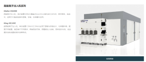
Three major Chinese semiconductor equipment firms Huahai Qingke, Naura Technology, and Lead Microelectronics’ subsidiary KST are accelerating domestic breakthroughs in ion implanters, a critical but long-monetized technology in chip manufacturing previously dominated by U.S. and European companies like Applied Materials and Axcelis (with $1.427 billion in 2024 imports).

KeyStone leads in rapid deployment, having delivered over 40 units by H1 2025, including 5+ million wafers via its 12-inch low-energy high-current implanter. It covers advanced logic, memory, power devices, and CIS with full-spectrum models and has passed key product validations (e.g., 28nm, dark current control).
1767020384398.png

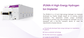
Huahai Qingke entered quickly through acquisition of Xinyu Semiconductor, launching its first 12-inch low-temperature implanter (iPUMA-LT) in July 2025 and showcasing a high-current model with advanced beam ramping. Leveraging existing CMP customer ties, it aims to replicate its success in front-end equipment.
1767020805291.png

Naura Technology, entering the market only in March 2025, boasts top-tier performance in accuracy, uniformity, and stability particularly in 3D NAND applications (beam efficiency >90%). With a planned 200-unit annual capacity starting in 2024 and partnerships with Yangtze Memory and Changxin, it targets high-end and emerging semiconductor needs.

1767020892981.png
Differentiated Pathways:

Technology:

KST emphasizes precision and modular design.
Huahai Qingke leverages integration via acquisition.
Naura relies on plasma/RF platform expertise for broad, high-end coverage.

Strategy:
KST focuses on niche mass production.
Huahai Qingke builds a "second growth curve" with existing customers.
Naura aims to become a full-front-end solution provider.

Ecosystems:
KST benefits from vertical integration.
Huahai from customer reuse and synergies.
Naura from deep industry partnerships and massive R&D investment (RMB 5.371 billion in 2024).
Market Outlook:

While imports still dominate, domestic production is gaining ground especially in low-energy high-current implanters. The next phase will focus on mass production capacity, customer trust, and verification in high-end applications (e.g., advanced logic, 3D NAND). To succeed against global competition, the three firms must collaborate on core component localization and technical standardization.

This "three-way battle" marks a pivotal shift toward China’s semiconductor industry self-reliance moving from isolated breakthroughs to a multi-pronged, competitive push for full control over front-end manufacturing.

Other companies:

SRI-I:
1767021190220.png

CETC Semicores:
1767021285804.png

Please, Log in or Register to view URLs content!
 

tokenanalyst

Lieutenant General
Registered Member

Norrico releases optical shape measurement equipment and delivers it to a leading domestic customer.​


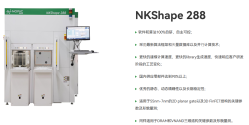
On December 26, Shanghai Norico Semiconductor Equipment Co., Ltd. (hereinafter referred to as "Norico") announced on its official WeChat account that the company recently launched a new product series: NKShape, an optical critical dimension (OCD) measurement device, and successfully delivered it to a leading domestic customer.

According to reports, the NKShape series of products is specifically developed for advanced semiconductor processes and is suitable for critical dimension measurement of complex structures such as Planar Gate, FinFET, DRAM, and 3D-NAND. Application scenarios include critical dimension measurement of two-dimensional or three-dimensional structures at process stations such as post-etching (ADI), post-etching (AEI), and post-chemical mechanical polishing (CMP), such as linewidth, trench depth, sidewall tilt angle, and specific material layer height at different locations.
1767021459218.png

Dr. Yuan Qiongyan, Chief Technology Officer of Norrico, introduced that Norrico's NKShape series of OCD metrology equipment provides the semiconductor metrology market with a high-quality OCD metrology device, thanks to its integrated system calibration, the latest algorithm architecture, and extensive experience in advanced processes. The NKShape series is based on metrology for 28nm/14nm process technology nodes, and can also cover critical dimension metrology for FinFET logic products, DRAM, and 3D-NAND memory products up to 7nm, 5nm, and more advanced processes.

Founded in 2022, Norric focuses on the design and development of front-end semiconductor metrology equipment. The company's core team comprises senior technical experts from the FaST division of a globally renowned semiconductor metrology equipment company. Leveraging its extensive experience serving numerous leading semiconductor manufacturers worldwide, Norric is committed to developing advanced OCD equipment.​

Please, Log in or Register to view URLs content!
 

tokenanalyst

Lieutenant General
Registered Member

Maiwei Technology: Providing Key Equipment Support for the Localization of HBM​


Maiwei Technology disclosed on its interactive platform that the company is optimistic about the domestic production prospects of high-bandwidth memory (HBM) technology. Its high-selectivity etching equipment and hybrid bonding equipment already possess the technical capabilities for application in DRAM (a core component of HBM) processes.

In response to investor inquiries, Maiwei Technology explicitly stated that its high-selectivity etching equipment and hybrid bonding equipment are adaptable to DRAM process stages, providing key equipment support for the domestic production of HBM. According to public data, as of the closing bell on December 27th, Maiwei Technology's stock price was 171.1 yuan per share, down 2.21% for the day, with a trading volume of 1.65 billion yuan, a total market capitalization of 47.8 billion yuan, and a price-to-earnings ratio of 54.06, indicating high trading activity.

As a core storage technology for AI chips, HBM's domestic demand is accelerating with the restructuring of the global semiconductor industry chain. Maiwei Technology, leveraging its accumulated expertise in core equipment technologies such as etching and bonding, has entered the DRAM process, aligning with the trend of domestic substitution.

If the localization of HBM accelerates, Maiwei Technology is expected to enter the memory chip market through equipment supply, expanding into a new growth engine beyond photovoltaic equipment. However, the risks of technology verification cycles and intensified industry competition need to be considered.

The company has not disclosed specific capacity plans but emphasized that it will continue to research and iterate equipment performance and strengthen technical collaboration with downstream customers to consolidate its first-mover advantage in the advanced packaging field.

Please, Log in or Register to view URLs content!
 

tokenanalyst

Lieutenant General
Registered Member

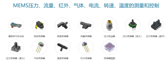
The CoreSense MEMS sensor chip industrialization project has been established in Changzhou, with an annual production capacity of over 200 million units.​

The CoreSense MEMS sensor chip industrialization project has been launched in Wujin National High-tech Industrial Development Zone, Changzhou, with an annual production capacity of over 200 million units. Wuxi XinGen Intelligent Technology Co., Ltd. and the zone have signed a cooperation agreement to establish a new R&D and manufacturing base focused on automotive and consumer electronics markets, with future expansion into humanoid robots and low-altitude economy applications.
1767028818221.png

The project, valued at 100 million yuan (with at least 50 million in fixed assets), will cover the full product lifecycle from chip design to testing and integration boosting XinGen’s independent supply capabilities. Wujin is advancing its "one person, one chip, one computing" industrial brand by hosting over 50 related projects, fostering a robust ecosystem that supports enterprise growth through ongoing service and investment.

Please, Log in or Register to view URLs content!
 

HighGround

Senior Member
Registered Member

Major domestic giants reshape the landscape of ion implanters.​


Three major Chinese semiconductor equipment firms Huahai Qingke, Naura Technology, and Lead Microelectronics’ subsidiary KST are accelerating domestic breakthroughs in ion implanters, a critical but long-monetized technology in chip manufacturing previously dominated by U.S. and European companies like Applied Materials and Axcelis (with $1.427 billion in 2024 imports).

KeyStone leads in rapid deployment, having delivered over 40 units by H1 2025, including 5+ million wafers via its 12-inch low-energy high-current implanter. It covers advanced logic, memory, power devices, and CIS with full-spectrum models and has passed key product validations (e.g., 28nm, dark current control).


Huahai Qingke entered quickly through acquisition of Xinyu Semiconductor, launching its first 12-inch low-temperature implanter (iPUMA-LT) in July 2025 and showcasing a high-current model with advanced beam ramping. Leveraging existing CMP customer ties, it aims to replicate its success in front-end equipment.


Naura Technology, entering the market only in March 2025, boasts top-tier performance in accuracy, uniformity, and stability particularly in 3D NAND applications (beam efficiency >90%). With a planned 200-unit annual capacity starting in 2024 and partnerships with Yangtze Memory and Changxin, it targets high-end and emerging semiconductor needs.


Differentiated Pathways:

Technology:
KST emphasizes precision and modular design.
Huahai Qingke leverages integration via acquisition.
Naura relies on plasma/RF platform expertise for broad, high-end coverage.

Strategy:
KST focuses on niche mass production.
Huahai Qingke builds a "second growth curve" with existing customers.
Naura aims to become a full-front-end solution provider.

Ecosystems:
KST benefits from vertical integration.
Huahai from customer reuse and synergies.
Naura from deep industry partnerships and massive R&D investment (RMB 5.371 billion in 2024).
Market Outlook:

While imports still dominate, domestic production is gaining ground especially in low-energy high-current implanters. The next phase will focus on mass production capacity, customer trust, and verification in high-end applications (e.g., advanced logic, 3D NAND). To succeed against global competition, the three firms must collaborate on core component localization and technical standardization.

This "three-way battle" marks a pivotal shift toward China’s semiconductor industry self-reliance moving from isolated breakthroughs to a multi-pronged, competitive push for full control over front-end manufacturing.

Other companies:

SRI-I:

So from what I read on the product page,

Sirius MC313 is for SiC 12 inch wafers. That's a frontier tool
The iPuma-H is also for power devices.

The KeyStone tools are the ones tripping me up. The iStellar says it's for mature 28/22 nodes and the iKing is a HE/UHE device (same application as iPuma-H then?). What would these be for? DRAM/NAND?
 

tphuang

General
Staff member
Super Moderator
VIP Professional
Registered Member
Please, Log in or Register to view URLs content!

So Lisuan Tech, who launched its 7G100 GPUs earlier this year using TSMC N6 process for cloud gaming, auto cockpit & such purposes, have delivered their chips to initial customers.

Remember that unlike Moore Threads, their scores on various GPU benchmark have been really good right from the start. Which means their firmware support is pretty good.
 

tokenanalyst

Lieutenant General
Registered Member

Domestic ATE breaks through! Aiming to break the monopoly of Advantest and Teradyne!​


Yuexin Technology, a Chinese semiconductor testing equipment company based in Hefei, officially began its A-share IPO process after completing listing guidance filing with the Anhui Securities Regulatory Bureau, with Huatai United Securities as the lead institution. This marks a major milestone in China’s push to break the global monopoly held by overseas ATE (Automatic Test Equipment) giants—Advantest (Japan) and Teradyne (U.S.), which together control about 80% of the global market.

Founded in 2017, Yuexin Technology has focused exclusively on developing high-end integrated circuit testing equipment. It has achieved significant technological breakthroughs with fully independent IP, including:
  • T800 series for SoC chips​
  • TP series for power semiconductors​
  • TM8000 series for memory chips​
1767045612199.png
These products have successfully filled critical gaps in China’s domestic ATE capabilities, achieving over 600 installations and serving more than 200 customers globally—ranging from design firms to research institutions.

Yuexin is recognized as a national-level "little giant" innovator, with over 60% of its workforce dedicated to R&D and more than 150 authorized or pending patents. It was previously included in the 2025UP China Hidden Unicorn 500 with a valuation of ¥5.2 billion.

With its upcoming IPO, Yuexin is poised to strengthen its domestic leadership and accelerate international expansion. The company’s success signals growing confidence in China's ATE industry and represents a key step toward reducing reliance on foreign suppliers, enhancing semiconductor supply chain security, and advancing China’s position in the global chip ecosystem.

Please, Log in or Register to view URLs content!
 

tokenanalyst

Lieutenant General
Registered Member

JCET Group successfully issued 2.4 billion yuan in technology innovation bonds to support the transformation of advanced packaging technology.​


Jiangsu Changjiang Electronics Technology Co., Ltd. (JCET Group) successfully issued RMB 2.4 billion in technology innovation bonds in 2025, marking the first phase of its authorized financing under a previously approved quota of up to RMB 4.8 billion over two years. The bond has a 5+5 year maturity and carries an interest rate of 2.00%, with Bank of Communications acting as lead underwriter.

The funds will be exclusively used to advance advanced packaging technology research and industrialization, supporting long-term technological innovation and R&D investment in the semiconductor sector.

This bond issuance reflects a key development in China’s tech-focused financial markets technology innovation bonds are designed to channel capital into high-tech enterprises with clear R&D commitments. The low interest rate underscores market confidence in JCET Group's technical capabilities and the future potential of advanced packaging in semiconductors.

Analysts view this as a signal of growing investor support for tech-driven industries under favorable macroeconomic conditions, highlighting the role of tailored bond instruments in fostering real economic innovation.​


Please, Log in or Register to view URLs content!
 
Top