Chinese semiconductor thread II

jx191

New Member
Registered Member
That writeup is still many times more constructive and useful than the Reuters article, however.
Definitely. That Reuters article is reporting on rumours and small bits of evidence all piled into one big headline.
If they knew what they were talking about, they'd realize that Chinese EUV has come a long way.
 

playmaker1478

Just Hatched
Registered Member
what is the status of SSMB euv? is that at back burner?
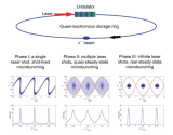
They are still in the experimental phase, currently conducting Proof-of-Principle Phase 2. The equipment was delivered to Metrology Light Source (MLS) in Berlin, with the goal of running by this quarter. We should be hearing more around 3-12 months regarding experimental verification.

Please, Log in or Register to view URLs content!


1766092409326.png
Picture taken from
Please, Log in or Register to view URLs content!
, page 120, to illustrate the goal of PoP Experiments.

In regard to facility in China, I believe they are under construction as it was recently approve.
 

sunnymaxi

Colonel
Registered Member
They are still in the experimental phase, currently conducting Proof-of-Principle Phase 2. The equipment was delivered to Metrology Light Source (MLS) in Berlin, with the goal of running by this quarter. We should be hearing more around 3-12 months regarding experimental verification.

Please, Log in or Register to view URLs content!


View attachment 166481
Picture taken from
Please, Log in or Register to view URLs content!
, page 120, to illustrate the goal of PoP Experiments.

In regard to facility in China, I believe they are under construction as it was recently approve.
construction has completed. now equipment installation is underway.

''Equipment procurement for the Steady-State Microbeam (SSMB) EUV Light Source Laboratory in Xiongan has begun''
 

tphuang

General
Staff member
Super Moderator
VIP Professional
Registered Member
Please, Log in or Register to view URLs content!

Article here about 华辰芯光 (huachen optoelectronics) using IDM approach for laser chips to be used in AI and space. It now has designed capacity of 20 million high power CW (continuous wave) laser chips. It's goals is realizing contactless FAB manufacture of 6-inch GaA and 4-inch InP chips. It has goals of adding more plant locations to increase production to 100 million per year to supply AI, satellites, military and Lidar markets.
 
Top