Shanghai Institute of Optics and Fine Mechanics has made progress in achieving metal-semiconductor edge contact through optical manipulation.
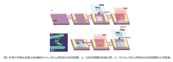
The Shanghai Institute of Optics and Fine Mechanics, Chinese Academy of Sciences, have developed a novel method to create metal-semiconductor edge contacts using optical manipulation with femtosecond lasers. This technique enables precise, fast, and damage-free movement of 2D nanosheets (MoTe₂ and NbS₂) on a dry substrate, allowing the fabrication of an edge-contacted MoTe₂–NbS₂ heterojunction photodetector.
Key advantages of this approach:
- Edge contact improves electron injection efficiency by eliminating Schottky barriers and reducing tunneling resistance.
- The device achieves high performance:
- Responsivity: 2 A/W
- Specific detectivity: 1.3 × 10⁸ Jones (at 900 nm)
- Ultrafast response: rise/fall times of 30/46 μs, bandwidth of 5.4 kHz
- Broad spectral detection from 280 to 1380 nm (or 1200 nm), enabling multi-wavelength sensing without complex calibration.
- Superior performance compared to traditional top-contact devices, which are limited by Schottky barriers and slow response times (seconds).
The method is efficient, cost-effective, and scalable, offering new pathways for designing high-performance optoelectronic devices—especially lateral heterojunctions with customizable edge structures. The study was published in Small as a back cover article and supported by China’s National Key R&D Program and National Natural Science Foundation.


