Chinese semiconductor thread II

tokenanalyst

Lieutenant General
Registered Member
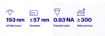
1 is the diffraction limit for dry lithography, ASML latest dry scanner variable from 0.70NA to .93NA but even if the twitter "Taiwanese" stooge says is true (he doesn't present any evidence) is irrelevant, dry litho is barely used today, the sale number from ASML are low. 0.85NA is capable of satisfying most of the needs in dry ArF lithography. The work horse of lithography are KrF and Immersion scanners.
The twitter guy seriously shows his lack of knowledge by citing the old 40W ArF excimer laser the RSLaser showcased in 2018, HARD evidence points out the RSLaser already has mastered 90W 6KHZ ArF immersion light source.

Twitter as most social media is crap for good information.
In case anyone wonder

.0.25 * (193/0.85)= 57nm

1762061473536.png

ASML doesnt even care.
What really matter is the overlay that for the 65nm was announced as 8nm below
Resolution / 3 = 57 / 3 = 19nm way above the 8-7nm that was announced
And yes that is the twitter stooge "insider", the Ministry of industry announcement and old 2018 news about RSLaser.
 

huemens

Junior Member
Registered Member
Nexperia China has send a letter to the customers. This letter is a response to the recent letter Nexperia Netherlands sent to customers informing the wafer cut off from their European fabs to China packaging facility.
Nexperia China letter further indicates they are increasing domestic wafer output.

Please, Log in or Register to view URLs content!
1. Nexperia's claim that "local management recently failed to comply with the agreed contract payment terms" is completely fabricated and maliciously smears Nexperia China's management. Nexperia China has not breached the contract; on the contrary, Nexperia currently owes ATGD as much as 1 billion RMB.
2. The relevant management of Nexperia in the Netherlands seriously neglected their duties and responsibilities in the decision-making process, putting personal interests above the overall interests of the company, and seriously violating professional ethics and corporate governance requirements. As a result, they should bear legal responsibility for the losses caused to the company and its employees.
4. Currently, Nexperia China has established sufficient finished goods and work-in-process inventory, enabling it to stably and continuously meet the order demands of its customers until the end of the year and beyond, ensuring a secure and reliable supply chain. To ensure the long-term sustainability and resilience of supply, we have proactively activated multiple contingency plans and are accelerating the verification of new wafer capacity. We are confident in completing verification in the short term and seamlessly meeting all customer needs starting next year.
 

spaceship9876

New Member
Registered Member
Samsung Falls from 2nd to 4th in Smartphone CIS Market Due to Surge of Chinese Competitors
Something that many of you might not know is that the EU has required smartphones to receive 5yrs of updates since june 2025 for all new models that go on sale after then. This will result in chinese companies having a much more similar number of updates to samsung and apple which will increase chinese smartphone marketshare in europe.
 

dropout003

New Member
Registered Member
And different from ASML. this supply chain could allow not only one but multiple companies competing, Like Naura with I-Line or KrF, SiCarrier, SMEE and CETC in ArF, Immersion and EUV. Different from ASML Chinese companies are more tolerant to work in the low margins pushing the price of lithography down. Also this lithography supply chain, as previous posts said, is already percolating in other areas. China sub-nanometer positioning technology is already being marketed for wafer inspection tools, EBeam litho, NIL and other areas.
Wafer stage for ebeam litho (+ other tools) from Yinguan showcased by their German partner.
Please, Log in or Register to view URLs content!
 

jx191

New Member
Registered Member
Temperature control for 5nm EUV nodes is ready.

View attachment 163682
Interesting to see that it is for 5nm nodes.
People discussed before about what node will be made first using EUV litho and I've always assumed that considering they have somewhat decent 5nm capabilities with DUV, they would want to make the jump to 3nm.
Maybe they are going to do their trials and testing for 5nm first, before going to 3nm? What does everybody else think?
 

tphuang

General
Staff member
Super Moderator
VIP Professional
Registered Member
Please, Log in or Register to view URLs content!

Great opportunity for both YMTC and CXMT to expand their production as the big 3 is fully booked until 2027 second half

This guy continues to see capacity not keeping up with demand well into 2027 and 2028. But I think he just has no idea how quickly Chinese memory fabs will expand.
 
Top