Explain please .. what is reservoir computing.Huawei is looking at reservoir computing. Might be an indicator of what direction they're going for.
Abstract
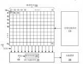
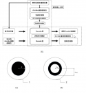
Reservoir computing originates in the early 2000s, the core idea being to utilize dynamical systems as reservoirs (nonlinear generalizations of standard bases) to adaptively learn spatiotemporal features and hidden patterns in complex time series. Shown to have the potential of achieving higher-precision prediction in chaotic systems, those pioneering works led to a great amount of interest and follow-ups in the community of nonlinear dynamics and complex systems. To unlock the full capabilities of reservoir computing towards a fast, lightweight, and significantly more interpretable learning framework for temporal dynamical systems, substantially more research is needed. This Perspective intends to elucidate the parallel progress of mathematical theory, algorithm design and experimental realizations of reservoir computing, and identify emerging opportunities as well as existing challenges for large-scale industrial adoption of reservoir computing, together with a few ideas and viewpoints on how some of those challenges might be resolved with joint efforts by academic and industrial researchers across multiple disciplines.
You are using an out of date browser. It may not display this or other websites correctly.
You should upgrade or use an alternative browser.
You should upgrade or use an alternative browser.
Chinese semiconductor thread II
- Thread starter vincent
- Start date
Jingsheng Electromechanical: 6-inch silicon carbide epitaxial equipment achieved volume sales and order volume grew rapidly
According to the company’s 2023 performance forecast announced on January 19, 2024, the company’s net profit attributable to shareholders of the listed company is 4,385,469,600 yuan – 4,970,198,900 yuan. This performance forecast data is the result of preliminary calculations by the company's financial department. It has not been pre-audited by an accounting firm. The specific financial data will be disclosed in detail in the company's 2023 annual report.
The company continues to promote the R&D and manufacturing of diamond wire slicer equipment technology, and has developed crystal slicing equipment in the three major fields of photovoltaic silicon, semiconductor silicon, and sapphire to meet the needs of high-quality slicing in multiple specifications from 4 to 12 inches. The production and sales are in good condition. On January 8, 2024, the Ministry of Industry and Information Technology and the State-owned Assets Supervision and Administration Commission of the State Council jointly announced the "one-stop" application demonstration direction and promotion organization list of key products and processes in 2023. The company serves as the application demonstration direction of "photovoltaic silicon wafer slicing technology and equipment" of promoting organizations were selected for this list.
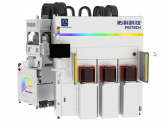
At present, the company has basically achieved full coverage and mass sales of 8-12-inch large silicon wafer equipment. The 6-inch silicon carbide epitaxial equipment has achieved mass sales and the order volume has grown rapidly. It has successfully developed an 8-inch monolithic device with internationally advanced levels. Silicon carbide epitaxial growth equipment realizes a mature and stable 8-inch silicon carbide epitaxial process. At the same time, based on the extension of the industrial chain, the company has developed thinning equipment, epitaxial equipment, LPCVD equipment, ALD equipment, etc. for 8-12-inch wafers and packaging.
The company has successively launched 6-inch dual-wafer silicon carbide epitaxy equipment and 8-inch silicon carbide epitaxy equipment. Among them, the 6-inch dual-wafer silicon carbide epitaxial equipment has achieved international leading advantages in terms of epitaxial production capacity and operating costs. Compared with single-chip equipment, the production capacity of a single dual-wafer equipment has increased by 70%, and the single-wafer operating cost has been reduced by up to 30%. The above helps customers create great value. The 8-inch silicon carbide epitaxy equipment is compatible with 6-inch and 8-inch silicon carbide epitaxy production, solving control problems such as temperature field uniformity and flow field uniformity in cavity design. The thickness uniformity of the epitaxy is within 1.5%, and the doping uniformity is within 1.5%. Within 4%, reaching the industry-leading level.
Domestic lithography machine parts have made breakthroughs, and Maolai Optics and Fujing Technology have led the industry change.
Maolai Optical's main products cover the full spectrum of deep ultraviolet DUV, visible light to far infrared, and mainly include three categories: precision optical devices, optical lenses and optical systems. Precision optical devices include lenses, prisms and flat films, which have the characteristics of high surface shape, high smoothness, and high-performance coating. They are used in major national strategic development fields such as photolithography machines, high-resolution satellites, lunar exploration projects, and civil aviation aircraft. The precision optical devices developed by the company have been used in domestic lithography machines, providing important support for the localization of lithography machines.
Fujing Technology's products are important components in the light source system for manufacturing lithography machines. It is in the upstream of the laser industry. The midstream mainly includes various lasers and supporting equipment, and the downstream mainly includes laser equipment and application equipment. The products are mainly used in the manufacture of solid-state, optical fiber and other types of lasers and are key components of laser systems. Some precision optical component products are used in optical communications, AR, lidar, semiconductor equipment, analytical instruments and other fields.
Fujing Technology's nonlinear optical crystals LBO and BBO account for nearly 80% of the market, ranking first in the world. Products are supplied to well-known domestic and foreign laser companies such as TRUMPF, Lumentum, and Raycus Laser. As the semiconductor industry continues to shift domestically, domestic semiconductor equipment parts and supply system manufacturers will usher in new development opportunities.
Interesting I-line laser for litho.
The Institute of Semiconductors has developed a GaN-based high-power ultraviolet laser with a continuous power of 4.6W at room temperature.
Gallium nitride (GaN)-based materials are called third-generation semiconductors. Their spectral range covers the full range of near-infrared, visible light and ultraviolet, and has important application value in the field of optoelectronics. GaN based
Gallium nitride (GaN)-based materials are called third-generation semiconductors. Their spectral range covers the full range of near-infrared, visible light and ultraviolet, and has important application value in the field of optoelectronics. GaN-based UV lasers have important application prospects in the fields of UV lithography, UV curing, virus detection, and UV communications due to their short wavelength, large photon energy, and strong scattering. However, because GaN-based ultraviolet lasers are prepared based on large mismatch heteroepitaxial material technology, they have many material defects, difficult doping, low quantum well luminous efficiency, and large device losses. This is a difficulty in the field of international semiconductor laser research and has been criticized at home and abroad. of great concern.
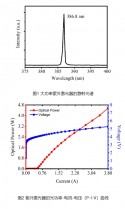
Researcher Zhao Degang and Associate Researcher Yang Jing of the Institute of Semiconductors, Chinese Academy of Sciences have long focused on the research of GaN-based optoelectronic materials and devices. In 2016, a GaN-based ultraviolet laser was developed [J. Semicond. 38, 051001 (2017)], and in 2022, an electrically injected lasing AlGaN ultraviolet laser (357.9nm) was realized [J. Semicond. 43,1 (2022)]. In the same year, A high-power ultraviolet laser with a continuous output power of 3.8W at room temperature [Opt. Laser Technol. 156, 108574 (2022)]. Recently, our team has made important progress in GaN-based high-power ultraviolet lasers, and found that the poor temperature characteristics of ultraviolet lasers are mainly related to the weak confinement effect of ultraviolet quantum wells on carriers. By introducing technologies such as the new structure of AlGaN quantum barriers, Significantly improve the temperature characteristics of high-power ultraviolet lasers, the room temperature continuous output power of ultraviolet lasers is further increased to 4.6W, and the lasing wavelength is 386.8nm. Figure 1 shows the lasing spectrum of a high-power ultraviolet laser, and Figure 2 shows the optical power-current-voltage (PIV) curve of the ultraviolet laser. Breakthroughs in GaN-based high-power UV lasers will promote the localization of devices and support the independent development of domestic UV lithography, UV curing, UV communications and other fields.

A wavelength-stabilized and quasi-common-path heterodyne grating interferometer with sub-nanometer precision.
Tsinghua Shenzhen International Graduate School, Tsinghua University, Shenzhen, ChinaAbstract:
Grating interferometers highly valued for high resolution, straightforward benchmark and insensitivity to environmental disturbances, have become one of the most mainstream methods for ultra-precision positioning. Traditional heterodyne grating interferometers which use a dual-frequency orthogonally polarized laser source suffer nanometer-level periodic nonlinear error due to frequency and polarization mixing, thus becoming incompetent to undertake sub-nanometer measurement. Based on the design of two separated laser beams with a small frequency difference for heterodyne beating, a wavelength-stabilized and quasi-common-path heterodyne grating interferometer is proposed. It incorporates a symmetrical oblique incidence structure where the residual dead path is calibrated and the laser source wavelength is stabilized to the rubidium atomic transition line, diminishing heterodyne phase errors resulted from the optical path difference. This approach not only significantly mitigates periodic nonlinear error to below 0.3 nm, but also enhances measurement resolution, repeatability and interference robustness. The proposed heterodyne grating interferometer is determined for ultra-precision positioning serving for precision machinery manufacturing and scanning beam interference lithography and so forth.
Grating interferometers highly valued for high resolution, straightforward benchmark and insensitivity to environmental disturbances, have become one of the most mainstream methods for ultra-precision positioning. Traditional heterodyne grating interferometers which use a dual-frequency orthogonally polarized laser source suffer nanometer-level periodic nonlinear error due to frequency and polarization mixing, thus becoming incompetent to undertake sub-nanometer measurement. Based on the design of two separated laser beams with a small frequency difference for heterodyne beating, a wavelength-stabilized and quasi-common-path heterodyne grating interferometer is proposed. It incorporates a symmetrical oblique incidence structure where the residual dead path is calibrated and the laser source wavelength is stabilized to the rubidium atomic transition line, diminishing heterodyne phase errors resulted from the optical path difference. This approach not only significantly mitigates periodic nonlinear error to below 0.3 nm, but also enhances measurement resolution, repeatability and interference robustness. The proposed heterodyne grating interferometer is determined for ultra-precision positioning serving for precision machinery manufacturing and scanning beam interference lithography and so forth.

