Chinese semiconductor thread II

gabriel.shenton

New Member
Registered Member
I'm afraid they will....and sooner more than later too: relying on Japan to resist is a big gamble, Japan politicians are totally dominated by US, even more than the European ones. Moreover they already did this trick with South Korea in the past, so there is a precedent.
Agreed, US has total control over G7's politicians and business elites, China is not only fighting 1 but 7 powerful opponents.

To protect Apple and Tesla, maybe Nvidia from Chinese competitions, US likely will do whatever it can to kneecap China's semiconductor industry.

I am rooting for Huawei's comeback(AI chips and mobile), but sanctions keep coming.
 

tokenanalyst

Brigadier
Registered Member

Hiwave domestic ultrasonic scanning microscope for Chuck inspection.​


Ultrasound has great advantages in detecting internal defects in ceramic composite materials. Compared with other detection methods, it has high detection sensitivity, accurate detection and imaging of area-type layered defects and welding quality. We can intuitively and accurately find the specific location of the defect. Ultrasonic SAM equipment has the advantages of accurate detection, high defect resolution, and intuitive imaging. Hiwave's ultrasonic scanning microscope supports layered scanning and tomography, which can conduct qualitative and quantitative analysis of defects, such as defect area, proportion and other characteristics. It is suitable for detecting various types of defects in ceramic materials, such as voids, cracks, bubbles, inclusions, delamination, welding, bonding, electroplating holes and other defects.

1709828053018.png1709829187733.png

Please, Log in or Register to view URLs content!
 

supersnoop

Major
Registered Member

Last year I was wondering if there's any domestic alternative to TI's DMD chips for projectors. Now there is a report saying that HiSilicon will soon release a LCOS solution for compact home projectors.
Please, Log in or Register to view URLs content!

Chinese projector makers have been very innovative at optics design, and both HiSilicon and Rockchip have SoCs for projectors. If HiSilicon can deliver on the crucial electro-optical steps then we'll have a whole supply chain safe from American control.
Isn't DMD a tiny, tiny market?

I believe that TI didn't even want to produce newer generations until there was a sudden uptick in demand for consumer short-throws in China in recent times. In fact, the classic home projector vendors (Epson, JVC, Optoma, Benq, though only the last two use DLP) have gone from facing less and less competition to suddenly having to face XGMI, Hisense, and Formovie along with numerous other Chinese upstarts along with LG.

Please, Log in or Register to view URLs content!
 

gelgoog

Lieutenant General
Registered Member
The lack of progress in replacing photoresist and other material imports is baffling to say the least. Maybe an export ban of photoresist from Japan is what it will take for the Chinese companies to get off their butt and start making and buying it local.
 

tokenanalyst

Brigadier
Registered Member
My personal view is the ASML situation is analogous to the TSMC situation. The US had to change the limit to technology limit to zero precisely because the governing jurisdictions (Netherlands and Taiwan respectively) were not going to put in voluntary restrictions and companies have creative accounting methods for determining the "US technology contribution". Iirc, TSMC at one point claimed 10% US technology amount when they dropped the limit. If the national governments would go ahead and implement restrictions voluntarily, there is no reason to change those parameters. The setting of the limit to zero is to serve as a de facto ban, regardless of whether the country of incorporation agrees to it. Now to save face the Dutch agree to comply, but the lowering of the limit to zero is basically a warning shot that if you don't take the steps the US government will do it for you by applying the block to ASML directly. As creative as your accounting and lawyers can be, with the structure of a company like ASML or TSMC there was no way you could claim zero US technology contribution.
I know the US treat the Europeans as their biggest lapdog, that they are the biggest cucks ever and they should be obedient. But the US is setting a precedent that could backfire really bad into US companies, what goes around comes around, the day will come that the US will want to export certain technology that the Europeans don't like to be exported to certain countries and with a zero export control policy they will have the power to block it. Imagine if the Europeans grow a pair and turn against Israel actions in Gaza and impose export controls to Israel, with ASML dominance is almost impossible to say that certain ICs have zero European contribution, imagine in a Trump administration if the Europeans turns against a Hawkish WH foreign policy. Imagine if Japan feud with South Korea comes back in full force and Japan decide to impose a zero export control policy. What goes around comes around.

One thing is for certain if this happen I would be rolling in the floor laughing so hard that my stomach will hurt.​
 

tokenanalyst

Brigadier
Registered Member
The lack of progress in replacing photoresist and other material imports is baffling to say the least. Maybe an export ban of photoresist from Japan is what it will take for the Chinese companies to get off their butt and start making and buying it local.
There are more companies entering the photoresist market than ever. Now covering I-line, KrF, ArF, ArFi and even some developing EUV. I will be pretty hard to make a resume of all the post previous thread but the they are advancing and expanding capacity pretty fast. If the Japanese give up and impose controls, it will give the government more impetus to accelerate their subsidies to expand photoresist production capacity and will accelerate the certification of China photoresist products.
 

gelgoog

Lieutenant General
Registered Member
There are more companies entering the photoresist market than ever. Now covering I-line, KrF, ArF, ArFi and even some developing EUV. I will be pretty hard to make a resume of all the post previous thread but the they are advancing and expanding capacity pretty fast. If the Japanese give up and impose controls, it will give the government more impetus to accelerate their subsidies to expand photoresist production capacity and will accelerate the certification of China photoresist products.
I always see the same talk from them. i.e. we are producing tiny amounts of legacy photoresists. we have prototype production of leading edge photoresists being sampled by customers. And then neither tiny production of leading edge photoresists happens, nor do they substantially scale up production of legacy ones. This has been happening for at least 5 years. Which you would think would be more than enough time to build factories and scale up photoresist production. For example there is more than one maker of KrF photoresist in China, and yet local production is only a tiny amount amount of the overall market.
 

tphuang

Lieutenant General
Staff member
Super Moderator
VIP Professional
Registered Member
for photoresist, Bokang only said Arfi photoresist has been qualified in the past year. I would just ignore Nata. They are irrelevant.

We don't know how much domestic production is as % of overall market. There is deliberate ambiguity here

Anyhow, more on SiC

Please, Log in or Register to view URLs content!
Gree will start it's 6 inch production line in June
looking to produce 240k wafers per year when fully ramped

Please, Log in or Register to view URLs content!
CR Micro says its SiC capacity is now up to 2500 wpm. This is steadily going up. 50% is used for SiC mosfet
 

sunnymaxi

Major
Registered Member
Fourth generation of semiconductor lighting technology ..

South China University of Technology has made new progress in research on high-power near-infrared light sources..

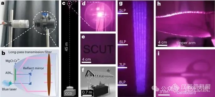
Introduction: Using an extremely simple MgO:Cr³⁺ near-infrared fluorescent transparent ceramic, a blue laser-driven near-infrared light source device was produced. The output power reached the current record high of 6 W, and its use in long-distance night vision supplementary light and Applications in non-destructive testing imaging and other fields.

Recently, Professor Xia Zhiguo's team from the State Key Laboratory of Luminescent Materials and Devices of South China University of Technology published a research paper titled "Laser-Driven BroadbandNear-Infrared Light Source with Watt-Level Output" online in the journal Nature Photonics . The paper reports on an extremely simple MgO:Cr³⁺ near-infrared fluorescent transparent ceramic. The output power of the blue laser-driven near-infrared light source device produced reached the current record high of 6 W, and demonstrated its long-distance night vision supplementation. Applications in areas such as light and non-destructive testing imaging.


36464143-4f4d-4757-834c-04c39a678605.jpg


Blue light-emitting diodes (LEDs) have given birth to the fourth generation of semiconductor lighting technology. New application requirements have put forward higher requirements for light source devices. Blue-light laser diodes (LDs) combined with fluorescent conversion materials have become an important development direction. It is made of extremely bright blue LD-pumped fluorescent conversion materials and has great potential in applications such as aviation and navigation lighting, underwater lighting, laser fluorescent display projectors, and high-power near-infrared light source devices.

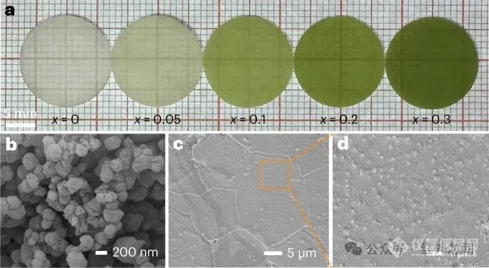
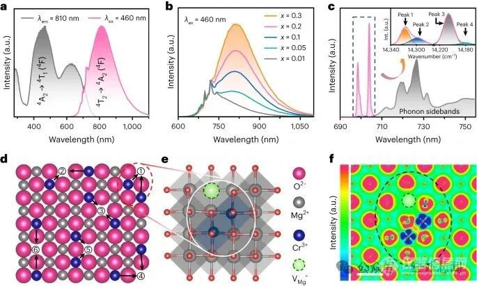
This research invented a highly stable MgO:Cr³⁺ fluorescent transparent ceramic that is close to "perfect performance" (Chinese invention patent, ZL202211147958.4). Its broadband near-infrared luminescence emission peak is 810 nm, achieving the highest external performance to date. Quantum efficiency (81%). The Cr³⁺ ions introduced through doping are heterovalently substituted at the Mg²⁺ lattice site, resulting in abundant cation vacancy defects in the structure, forming Cr³⁺ luminescence centers with different local environments. At the same time, the phonons between the luminescent centers assist the excited state energy transfer process, which compensates for the non-radiative relaxation of long-wavelength emission, overcomes the influence of energy gap ratio, and improves the luminous efficiency. Further benefiting from the ultra-high thermal conductivity of MgO fluorescent transparent ceramics, a broadband near-infrared output power of more than 6 W was obtained under 22 W/mm² blue LD pumping, with a light conversion efficiency of 29%.

153bfc6c-dc23-4601-b22d-65b6c2244410.jpg


The prototype device built using this technology can penetrate 3 cm thick opaque cardboard and achieve imaging of the scissors model, with an imaging resolution of 6l p/mm. This new laser-driven high-power near-infrared light source has broad application prospects in the fields of night vision supplementary light, industrial flaw detection equipment, and non-destructive testing imaging of medical devices.

d379bcb7-9b0e-4803-83e5-5e768fda17dc.jpg


Please, Log in or Register to view URLs content!
 
Top