i think we missed this news ..
Ten years of sharpening the sword! Professor Wang Hongxing’s team at Xi’an Jiaotong University achieved mass production of 2-inch single crystal diamond electronic devices..
As a representative of the third generation of semiconductor materials, diamond semiconductor is also called the ultimate semiconductor. “Diamond semiconductor has material properties such as ultra-wide bandgap (5.45eV), high breakdown field strength (10MV/cm), high carrier saturation drift velocity, high thermal conductivity (22 W/cmK), and excellent device quality. Factor." Professor Wang Hongxing of Xi'an Jiaotong University introduced, "To this end, the use of diamond substrates can develop high-temperature, high-frequency, high-power, radiation-resistant electronic devices, and overcome technical bottlenecks such as the 'self-heating effect' and 'avalanche breakdown' of the device. , playing an important role in the development of 5G/6G communications, microwave/millimeter wave integrated circuits, detection and sensing and other fields." However, the development of diamond electronic devices around the world is limited by the problem of large-size, high-quality single crystal substrates.
"The commercialization of silicon, sapphire and other substrates has provided prerequisites for heteroepitaxial single crystal diamond." Wang Hongxing said.
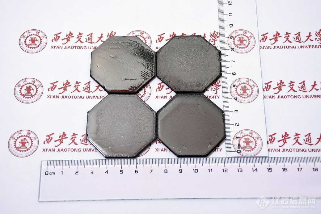
Recently, the team of Professor Wang Hongxing of Xi'an Jiaotong University used independent research and development technology to successfully achieve mass production of 2-inch heteroepitaxial single crystal diamond self-supporting substrates.
While Wang Hongxing led the team to tackle key research and development problems in the laboratory, he also carried out extensive cooperation in the research and development and application of diamond semiconductor materials and devices with relevant large domestic communication companies and relevant research institutes of China Electronics Technology Group, promoting the development of diamond RF power electronic devices, power electronic devices, Practical development of MEMS and other devices. Wang Hongxing's team used microwave plasma chemical vapor deposition (MPCVD) technology to successfully mass-produce 2-inch heteroepitaxial single-crystal diamond self-supporting substrates, and through effective control of film formation uniformity, temperature field and flow field, and then The yield of heteroepitaxial single crystal diamond is improved. The substrate surface has a step-flow growth mode, which can reduce the defect density of the substrate and improve the crystal quality. The half-peak widths of XRD (004) and (311) rocking curves are less than 91arcsec and 111arcsec respectively. All indicators have surpassed the best foreign standards and reached the world's leading level.