
You are using an out of date browser. It may not display this or other websites correctly.
You should upgrade or use an alternative browser.
You should upgrade or use an alternative browser.
Chinese semiconductor industry
- Thread starter Hendrik_2000
- Start date
- Status
- Not open for further replies.
SMIC revenue up 4% compared with the last quarter.

They have more Chinese client and less US clients, this contradict the idea that Huawei is making their chips alone.

The auto and power electronics sector taking bigger share.

They have more Chinese client and less US clients, this contradict the idea that Huawei is making their chips alone.
The auto and power electronics sector taking bigger share.
Just to clarify, these aren't related to "integration testing", but patents for auxiliary usability features you would include in a product that's intended to be commercially competitive.First we've seen the laser calibration, now we've got the optics. What's next on the list for integration testing?
That was my general understanding as well. This patent sounds like a secondary capability or feature to integrate multiple steps and workflows around a single light source infrastructure. Would be pretty neat if they completely redefine the EUV production flow. Of course it's all speculative until it's actually done.-in a first aspect of the present invention, a mask defect inspection apparatus is provided, including: the mask to be detected is arranged in the vacuum cavity, and an injection port and an ejection port through which an extreme ultraviolet light beam passes are arranged on the shell
-In a second aspect of the present invention, a mask defect inspection system is provided, where the mask defect inspection system includes: a plurality of mask defect inspection devices according to the first aspect;
- In a third aspect of the present invention, a lithography system is provided, including: the mask defect detecting system in the second aspect solution; and each photoetching machine is communicated with one sub-beam output pipeline in the mask defect detection system, and an extreme ultraviolet light emitting device in the mask defect detection system supplies an extreme ultraviolet beam to the photoetching machine through a light splitting device.
Also the picture of the patent is oddly similar to this:
View attachment 121164
A EUV projection objective, which its main function is to project the reduced image of the EUV mask into the coated wafer.
The emphasis on mask inspection is probably more due the lack of euv pellicles.
It looks like they are using this device as an EUV patterning device and EUV metrology tool, makes logic, SSMB and FELs are so powerful that could probably power multiple of these devices in a row, for both metrology and patterning.
Yeah, the idea of a "EUV lithography factory" that the media has been throwing around doesn't seem far fetch. We would have to wait until the first public FEL-SSMB powered experimental fabs come around.Just to clarify, these aren't related to "integration testing", but patents for auxiliary usability features you would include in a product that's intended to be commercially competitive.
That was my general understanding as well. This patent sounds like a secondary capability or feature to integrate multiple steps and workflows around a single light source infrastructure. Would be pretty neat if they completely redefine the EUV production flow. Of course it's all speculative until it's actually done.
It's the most sensible way to work around the physical footprint of a particle accelerator based light source and the production economy effects that bring. But I think it also means that there's a lot more to commercial adoption and utilization than "we got a scanner working".Yeah, the idea of a "EUV lithography factory" that the media has been throwing around doesn't seem far fetch. We would have to wait until the first public FEL-SSMB powered experimental fabs come around.
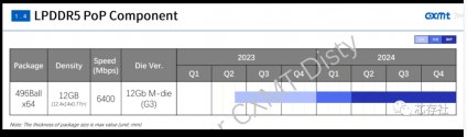
Nice, although still waiting for it to actually happening to breathe a sign of relief. Looks like if manufacturing can start in Q2, then maybe it can make it into Huawei supply chain in 2nd half of 2024Cxmt lpddr5 roadmap
i believe 1 is mosfet and the other is diode. But more importantly, Ziener is a company looking to find customers for a new product whereas CAS is doing more for research reasons. After CAS does its invention, there is still a process toward putting it into production which requires companies to be created (if I understand the Chinese model correctly).CAS has already made the breakthrough in 1200V GaN-on-Si diode in 2022. Is this a different kind of diode from Ziener?
just for the longest time, people didn't think we need 1200 GaN power modules. So, I'm interested to see what's changed.
In fact, Innoscience doesn't have any 800V+ product in its lineup and it's far and away the worlds largest GaN power chip maker
Let see what happens, necessity is the mother of inventions.It's the most sensible way to work around the physical footprint of a particle accelerator based light source and the production economy effects that bring. But I think it also means that there's a lot more to commercial adoption and utilization than "we got a scanner working".
Dinglong Co., Ltd. has been approved for a number of major photoresist-related projects and will receive financial support of approximately 160 million yuan.
On the evening of November 9, domestic semiconductor materials manufacturer Dinglong Co., Ltd. announced that the company and its subsidiaries have received a number of national and provincial important project notifications related to photoresist this year. The company's three major areas of photolithography are: Glue-related products: Integrated circuit wafer photoresist and core raw materials, semiconductor advanced packaging photoresist, and semiconductor flexible display photoresist-related projects will receive project funding support of no more than 164 million yuan in total.


- Status
- Not open for further replies.