They can really take market share from them, if they don't put aside their arrogance.Hi mderfox,
Cause SMEE had already develop a more advance 28nm DUVL, which means their DUVL product is redundant and expensive to maintain compare to SMEE. The only chance for ASML to be relevant in China is to sell them their EUVL, they had to be quick, within a year or two even that opportunity will be lost as SMEE will launching its own EUVL.
You are using an out of date browser. It may not display this or other websites correctly.
You should upgrade or use an alternative browser.
You should upgrade or use an alternative browser.
Chinese semiconductor industry
- Thread starter Hendrik_2000
- Start date
- Status
- Not open for further replies.
As I report in my book, Scanlan explained what AI would do for manufacturing. "Let's take robotics today," he told me. "5G changes everything. Typically, 5G is spoken about in terms of download speed, but that's not the most important advantage. For industrial processes, autonomous vehicles and other applications, the latency—the time it takes for one device to acquire and respond to a signal from another device—is more important. On a factory floor today, Robot A does its instruction, passes the bit to Robot B, and it's the same thing. Now, if we put very low latency inside each of the robots—and they can be robots from different manufacturers—and put them in a room and give them the rules, like Go or like chess, to enable them to connect in real time—milliseconds, lightning fast—and then put a bit of plastic in view and say, I want you to make a plastic cup, the robots will organize themselves much better than we would have thought."
This guy has no clue about general business and manufacturing, and definitively has no clue about robots and automation.
This sounds like something that a teenager wrote who fall in love with Euclid's Elements, and think that the whole world can be simplified into propositions and proofs deducted from few simple postulates .
Its hard to describe how wrong on so many level .
Maybe the Provident tech update wasn't screwed up, all that they missed was the 5G
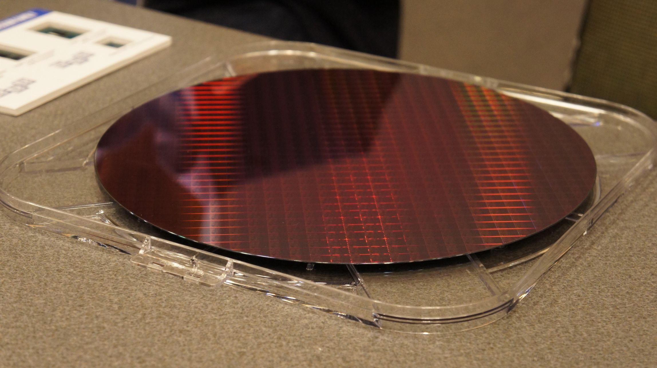
Question for the experts, what is the significant of this development, from my understanding most leading edge FABS industry including SMIC use 12 inch wafer for Chips production.
from cnTechPost
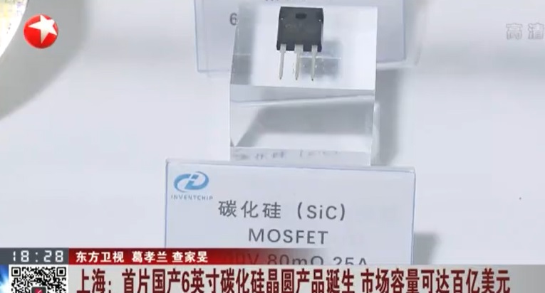
First China-made 6-inch silicon carbide wafer released in Shanghai
2020-10-17 21:09:21 GMT+8 | cnTechPost
0

The first China-made 6-inch silicon carbide MOSFET (metal oxide field effect transistor) wafer was released in Shanghai on October 16, according to a report by the local Oriental Satellite Television.
The 6-inch silicon carbide MOSFET wafer is based on silicon carbide (third-generation semiconductor material) and is used in new energy industries such as new energy vehicles and photovoltaic power generation.

Zhang Yongxi, founder and general manager of Shanghai Inventchip Technology, which manufactured the wafer, said: "If a silicon carbide MOSFET new energy vehicle is used for electric drive, the mileage can be improved by 5 to 10 percent."
For example, if you use a photovoltaic inverter with silicon carbide process devices, the efficiency can also be very much improved especially in the energy consumption is reduced by 50%, he said.
Inventchip Technology, a high-tech chip company focused on silicon carbide (SiC) semiconductors, was founded in 2017 in the new Lingang district of the Shanghai Free Trade Zone.
After three years of research and development, it became the first company in China to master the 6-inch SiC MOSFET and SBD processes, as well as SiC MOSFET driver chips, the company said.
from cnTechPost
First China-made 6-inch silicon carbide wafer released in Shanghai
2020-10-17 21:09:21 GMT+8 | cnTechPost
0

The first China-made 6-inch silicon carbide MOSFET (metal oxide field effect transistor) wafer was released in Shanghai on October 16, according to a report by the local Oriental Satellite Television.
The 6-inch silicon carbide MOSFET wafer is based on silicon carbide (third-generation semiconductor material) and is used in new energy industries such as new energy vehicles and photovoltaic power generation.

Zhang Yongxi, founder and general manager of Shanghai Inventchip Technology, which manufactured the wafer, said: "If a silicon carbide MOSFET new energy vehicle is used for electric drive, the mileage can be improved by 5 to 10 percent."
For example, if you use a photovoltaic inverter with silicon carbide process devices, the efficiency can also be very much improved especially in the energy consumption is reduced by 50%, he said.
Inventchip Technology, a high-tech chip company focused on silicon carbide (SiC) semiconductors, was founded in 2017 in the new Lingang district of the Shanghai Free Trade Zone.
After three years of research and development, it became the first company in China to master the 6-inch SiC MOSFET and SBD processes, as well as SiC MOSFET driver chips, the company said.
Well, it is significant, but this isn't something you will use to make SoCs for smartphones or servers. You won't make a CPU with this.
Low power electronics like that typically use either bulk silicon (Si) or silicon on insulator technology (SOI).
SiC (silicon carbide) is usually used for high-power electronics which regular Si (silicon) can't handle all that well.
So yes this is something for inverters and other high power applications. Maybe high powered radar or microwave too.
Typically there isn't as much demand for products which use SiC as Si so they typically use smaller wafers. The article above for example basically describes them using the wafers to produce discrete transistors not complex designs.
Last edited:
hi gelgoog,Well, it is significant, but this isn't something you will use to make SoCs for smartphones or servers. You won't make a CPU with this.
Low power electronics like that typically use either bulk silicon (Si) or silicon on insulator technology (SOI).
SiC (silicon carbide) is usually used for high-power electronics which regular Si (silicon) can't handle all that well.
So yes this is something for inverters and other high power applications. Maybe high powered radar or microwave too.
Typically there isn't as much demand for products which use SiC as Si so they typically use smaller wafers. The article above for example basically describes them using the wafers to produce discrete transistors not complex designs.
thanks for explaining it in layman term, learn a lot.
So I read this thread on twitter saying that focusing ONLY on smartphone/pc SoC as semiconductor OKR is not a good idea. There are a lot of semiconductor products beyond that and they can be manufactured by indigenously right now.Well, it is significant, but this isn't something you will use to make SoCs for smartphones or servers. You won't make a CPU with this.
Low power electronics like that typically use either bulk silicon (Si) or silicon on insulator technology (SOI).
SiC (silicon carbide) is usually used for high-power electronics which regular Si (silicon) can't handle all that well.
So yes this is something for inverters and other high power applications. Maybe high powered radar or microwave too.
Typically there isn't as much demand for products which use SiC as Si so they typically use smaller wafers. The article above for example basically describes them using the wafers to produce discrete transistors not complex designs.
Hi TD739,
Typical American thinking of what's gonna happen with China chip drive.
What does rapproachment mean? Back to old self normal and happy dandy?
Well its obvious, their strategy failed. A reset will happen alongside China drive for self sufficiency. Lets be realistic it takes a minimum of 2 years for China replacement to mature and China is pragmatic enough to accommodate some Western request. But no question, this sanction had indoctrinate the Chinese industries the importance of self reliance.
The question why it takes some serious hard hitting by US to wake up China?Hi TD739,
Well its obvious, their strategy failed. A reset will happen alongside China drive for self sufficiency. Lets be realistic it takes a minimum of 2 years for China replacement to mature and China is pragmatic enough to accommodate some Western request. But no question, this sanction had indoctrinate the Chinese industries the importance of self reliance.
Right now China emphasis is complete.domestic made equipments for mature tech.
Well, shouldn't they be prepared even before tech war begin. At least full domestic 45nm tech for military industrial complex, no?
China didn't bother to do that for military industry. What's wrong?
I thought Xi is total self reliant guy.
While China was indulged in some kind of esctasy, it was Trump given the credit to wake up China
Last edited:
- Status
- Not open for further replies.
