Chinese semiconductor industry

Status
Not open for further replies.

curiouscat

Junior Member
Registered Member
Please, Log in or Register to view URLs content!

HIKSEMI 1TB 2TB M.2 SSD 2230 NVMe PCIe Gen 4x4 SSD for Steam Deck ROG FLOWZ13 Surface ProX Laptop
Please, Log in or Register to view URLs content!
IMG_2365.jpeg
Hiksemi’s 2230 NVME launched globally a little bit later than they originally planned to. Looks like they also upgraded the 1TB version to Xtacking 3.0 232 which I didn’t expect.

By far the fastest 2230 NVME SSD available.
 

BoraTas

Captain
Registered Member
I mean this is Taiwan we are talking about here. what do they possibly have for 14nm manufacturing tech that the mainland does not?

It's just nonsense

Taiwan's semiconductor manufacturing is almost completely dependent on foreign upstream inputs and American fabless designers. Which is also why "China wants Taiwan for semiconductors" is a huge nonsense.
 

tokenanalyst

Brigadier
Registered Member

Xinlian Integration: 8-inch silicon-based production capacity is 170,000 pieces/month, and the products have been supplied to most new energy vehicle brands​


Xinlian Integration (formerly SMIC) stated on the investor interactive platform that as of the end of the third quarter, the company’s monthly production capacity of 8-inch silicon had reached 170,000 pieces; SiC MOS, 12-inch silicon The basic test line is also in the process of ramping up production. According to the current plan, the company's 12-inch silicon-based wafer production capacity is expected to reach a production capacity of 100,000 pieces/month in the future. After all the above-mentioned projects are fully completed, the company is expected to achieve a monthly production capacity of about 400,000 8-inch wafers (note: one 12-inch wafer is equivalent to 2.25 8-inch wafers).

Xinlian Integration also stated that as an open core chip foundry platform, the company can provide all types of customers with one-stop system foundry services from wafer manufacturing, module packaging, application verification to reliability testing. The customers the company cooperates with It includes not only chip design companies, but also system manufacturers and terminal host manufacturers. At present, the company's products have been applied to most new energy vehicle brands in the current market through various channels.

Please, Log in or Register to view URLs content!
 

tokenanalyst

Brigadier
Registered Member

Xuzhou Semiconductor Industry Association was established​


The founding meeting of the Xuzhou Semiconductor Industry Association was held in Xu recently. Zhang Xingwang, deputy director of the Xuzhou Municipal Bureau of Industry and Information Technology, Zhao Tao, director of the Social Organization Management Office of the Municipal Civil Affairs Bureau, and Hao Chunyi, director of the Information Industry Division of the Municipal Bureau of Industry and Information Technology, Ma Chunxi, deputy director of the Military Science and Technology Quality Department of the 46th Research Institute of China Electronics Technology Group Corporation, and others attended the meeting. Relevant leaders of the association's member units also attended the meeting. The general meeting elected the members of the first council of the association. Tian Xin, president of Jiangsu Xinhua Semiconductor Technology Co., Ltd., was elected as the first chairman of the association.

The Xuzhou Semiconductor Industry Association is a city-wide, industry-based, non-profit social group voluntarily formed by Xuzhou semiconductor-related enterprises, scientific research institutions, universities and other units under the guidance of the Xuzhou Municipal Bureau of Industry and Information Technology. The establishment of the association aims to promote the development of the semiconductor industry in Xuzhou, strengthen exchanges and cooperation between enterprises, and promote industrial upgrading and technological innovation.

Zhang Xingwang emphasized that the semiconductor industry is of great significance to the national strategic development. It is a strategic, basic and leading industry, and is the main battlefield for countries to compete in the field of scientific research. The establishment of Xuzhou Semiconductor Industry Association is in line with the needs of economic development and situation, and it is the right time. When referring to the current development status of the semiconductor industry in Xuzhou City, Zhang Xingwang said that since the release of the "Implementation Plan for the Development of Integrated Circuits and ICT Industry" in October 2017, Xuzhou City has gradually formed a strategy of taking materials and equipment as its advantages and moving towards packaging, testing, and design. , manufacturing-extended industrial clusters, focusing on key areas such as semiconductor materials, semiconductor equipment, advanced semiconductor packaging and testing, third-generation semiconductor materials and devices, and terminal applications, have created a large number of industry-leading highlights in segmented tracks.

Tian Xin, the first chairman of the association, pointed out in his speech that Xuzhou City has achieved more differentiated and characteristic innovative development with semiconductor materials as the starting point and semiconductor polysilicon and equipment as the breakthrough point. Xinhua Semiconductor's electronic-grade polysilicon, Zhonghuan's large silicon wafers, Yingsu's photolithography machines, Bocon's photoresists, and Leuven's etching machines have achieved domestic leadership in the segmented fields. In the future, the association will give full play to its role as a bridge, integrate platform resources, closely unite all member units, fully carry out policy research and technical exchanges, actively provide suggestions for government decision-making and industrial development, and jointly build the association into a high-level industrial chain docking and exchange platform , to promote the rapid and healthy development of the city’s semiconductor industry.
 

tokenanalyst

Brigadier
Registered Member

Banlun Electronics (Primarius): Participated in the establishment of a special EDA industry investment fund to promote the construction of the domestic EDA ecosystem​

Banlun Electronics released a record of investor relations activities and disclosed that the company participated in the establishment of an EDA special industry investment fund with its own funds, and received support from Shanghai Lingang, Zhangjiang Hi-Tech and Xingcheng Capital, a well-known semiconductor investment institution. Great support. At present, the special industrial investment fund is still completing the industrial and commercial registration procedures and signing of relevant documents.

Banlun Electronics said that by participating in the special industry investment platform in the direction of the EDA industry chain, the company can make full use of the respective advantages of the industry investment platform partners, pool the resource endowments of all parties, and find EDA industry chain investments with high technology content and high growth potential. Invest in the target to further promote the company's business expansion and technical cooperation in the EDA field, accelerate the construction of the domestic EDA ecosystem, and make a strategic layout for the company's sustainable development. The domestic EDA industry is still in the early stages of development due to the relatively lagging development and support of the industry's ecological environment. This has led to the current situation of a large number of EDA startups and a fragmented competitive landscape. However, the active EDA primary market has also provided opportunities for the Chinese EDA industry. The development soil not only reflects the high attention paid to domestic EDA software, but also creates a window of opportunity for the integration and linkage between local EDA companies.

Please, Log in or Register to view URLs content!


tphuang

Lieutenant General
Staff member
Super Moderator
VIP Professional
Registered Member
HLMC took over GF Chengdu. Another advanced node fab??

Please, Log in or Register to view URLs content!
makes sense for them to get into 14nm here. 30k wpm is decent amount of capacity

Xinlian Integration: 8-inch silicon-based production capacity is 170,000 pieces/month, and the products have been supplied to most new energy vehicle brands​


Xinlian Integration (formerly SMIC) stated on the investor interactive platform that as of the end of the third quarter, the company’s monthly production capacity of 8-inch silicon had reached 170,000 pieces; SiC MOS, 12-inch silicon The basic test line is also in the process of ramping up production. According to the current plan, the company's 12-inch silicon-based wafer production capacity is expected to reach a production capacity of 100,000 pieces/month in the future. After all the above-mentioned projects are fully completed, the company is expected to achieve a monthly production capacity of about 400,000 8-inch wafers (note: one 12-inch wafer is equivalent to 2.25 8-inch wafers).

Xinlian Integration also stated that as an open core chip foundry platform, the company can provide all types of customers with one-stop system foundry services from wafer manufacturing, module packaging, application verification to reliability testing. The customers the company cooperates with It includes not only chip design companies, but also system manufacturers and terminal host manufacturers. At present, the company's products have been applied to most new energy vehicle brands in the current market through various channels.

Please, Log in or Register to view URLs content!
yep, 芯联集成 (formerly SMEC) is the leader in China for power chips for EV
 

tokenanalyst

Brigadier
Registered Member

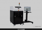
Uripu SiC doping measurement equipment SICV200 shipped to two customers.​


Urupa Semiconductor Equipment (Wuxi) Co., Ltd. ("Urupup" for short) has achieved great results again! Recently, the company announced the successful launch of the wafer resistivity measurement equipment SICV200. Currently, two customers have been shipped at the same time!

SICV200 is a semiconductor measurement equipment used to measure the resistivity of silicon wafers and the doping concentration of silicon carbide or other semiconductor materials. It can support sustained multi-frequency CV on wafers of various sizes including 12 inches. Characterization analysis. In terms of machine configuration, SICV200 has semi-automatic solutions of various sizes and fully automatic solutions that comply with SEMI standards. It can be directly connected to the customer's factory MES system to achieve automated production.​

1702133699424.png

Urupu film thickness measurement equipment successfully delivered​

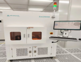
The Eos200 DSR is a fully automated equipment compatible with 8/6-inch wafer sizes and used to measure the thickness of multi-layer films of different materials on the surface of SOI (Silicon-On-Insulator) wafers. One application is the simultaneous measurement of silicon dioxide (BOX) and a wide range of top silicon thicknesses on SOI wafers. Eos200 DSR can measure the top silicon thickness from less than 1 micron to hundreds of microns while measuring BOX from tens of nanometers to several microns.

1702134131206.png

This equipment can also be applied to the thin film measurement requirements of other materials, such as the newly emerging silicon-based lithium niobate.
Eos200 DSR (6&8-inch wafer) and Eos300 DSR (12-inch wafer) are fully automatic solutions that fully comply with SEMI standards and can be directly connected to the customer's factory MES system to achieve automated production.

Previously, Urupu has successively launched a series of semiconductor-specific FTIR (Fourier transform infrared spectroscopy) measurement equipment:
  • Suitable for silicon-based epitaxial layer thickness measurement equipment Eos200/Eos300
  • Applicable to silicon-based element concentration (B/P/F) measuring equipment Eos200+/Eos300+
  • Through optimized hardware design (updated infrared spectrometer technology) and independently developed algorithms, the Eos200L, a silicon carbide (SiC) epitaxial layer thickness and epitaxial buffer layer thickness measurement equipment, is realized
  • Through optimized hardware design (updated infrared spectrometer technology) and self-developed Global Fitting Algo. TM algorithm technology, silicon carbide multi-layer (≥3 layers) epitaxial film thickness measurement equipment Eos 200L+ is realized
  • Helios, a device for measuring C/O content in silicon materials
  • The SICV200 wafer resistivity measurement equipment released by Urupu not only achieves the test performance of fully benchmarking foreign suppliers, but also completes the goal of localization of the equipment supply chain.

Please, Log in or Register to view URLs content!
 
Status
Not open for further replies.
Top