Chinese semiconductor industry

Status
Not open for further replies.

tokenanalyst

Brigadier
Registered Member
Building an ALD+CVD dual technology platform, a variety of CVD equipment has been launched.

The company has formed a system with ALD technology as the core and CVD and other vacuum coating technologies as a step-by-step development system. Products include ALD, PECVD, LPCVD equipment, etc. In terms of ALD equipment, both TALD and PEALD have mature models, and have developed a variety of deposition materials. They have received orders in the fields of logic, storage, compounds, and new displays, and are expected to continue to bloom in the future. A variety of CVD equipment has been launched. PECVD equipment can deposit SiO2, SiN, Lok, etc., and LPCVD equipment can deposit SiGe, p-Si, dopeda-Si, SiO2, SiN, etc. The first CVD equipment has been shipped to the client in July 2023.

Please, Log in or Register to view URLs content!
 

tokenanalyst

Brigadier
Registered Member

Up to 30 million, Beijing’s High-Precision Industry Development Fund Implementation Guidelines (Second Batch) Released​


On the evening of the 25th, the Beijing Municipal Bureau of Economy and Information Technology issued the "2023 Beijing High-Precision Industry Development Fund Implementation Guidelines (Second Batch)" notice, which this time involves new intelligent computing chips, new memories, open source processors, silicon The first round of optical chip production.

According to the announcement, there are four areas and directions of focus support this time. The first one is the first-round tape-out reward for integrated circuit design products, which supports integrated circuit design companies to carry out multi-project wafers (MPW) or the first-round tape-out of engineering products ( Full mask), qualified companies will be rewarded according to a certain proportion of tape-out costs, and the annual reward amount for a single company shall not exceed 30 million yuan.

The first key direction is the first round of tape-out of integrated circuit design products. The applicant for this direction must be an industrial and software information service enterprise registered in Beijing , with independent legal person qualifications , and engaged in the integrated circuit design business . On April 1, 2023 The first round of multi-project wafer (MPW) or engineering product tape-out (full mask) will be carried out between October 31, 2023, and the product tape-out contract has been completed, and the company has committed to carry out the industrialization of the product in Beijing.

Please, Log in or Register to view URLs content!
 

Weaasel

Senior Member
Registered Member
@tphuag, With all due respect, I still think it's important I comment on @Weaasel's question. If you still think this is not good for this thread, feel free to remove this post.

I think everybody paid too much attention to litho tool as the bottleneck, and recently are giving lots of attention to the progress domestic WFE suppliers are making on etcher, deposition, wet process equipment, resists, and even EUV light source. I don't think people realize there are still many big gaps to fill in order to break the US restriction on advanced logic/DRAM/3D-NAND IC fabrication. Don't take my word at face value, I encourage you to investigate the list below to validate my concerns.

Potential bottleneck to reach self-sufficiency for Advanced Technology Nodes
Wafer:

Bright field wafer inspection
Dark field wafer inspection
ebeam inspection
diffraction based ADI Overlay metrology
AEI overlay metrology
CD SEM

Reticle:
advanced domestic merchant maskshops
reticle blanks
ebeam reticle writer
reticle etcher (Chrome & MoSi)
reticle blank inspection (should be relatively easy to overcome)
reticle inspection
reticle CD SEM
reticle registration metrology
reticle repair tool
AIMS
pellicles
curvilinear OPC for EUV reticles
multibeam reticle writer for EUV
EUV reticle blanks
EUV pellicle

Maybe it's just me, but I couldn't find much information on domestic WFE working on the above toolsets for <=16nm logic / <=18nm hp DRAM / >=128L 3D-NAND. Now that I've brought this to everyone' attention, perhaps you all could keep an eye out for relevant news or info. With more people looking it may be faster for us to verify where we sit relative to advanced node needs. Note, we still have access to advanced reticles from the Japanese maskshops, the reticle fabrication equipment I outlined would only come into play as bottleneck if the U.S. blocks sale of advanced reticles to China.
That's a lot of vulnerability...
 

Didida

New Member
Registered Member
HiSilicon: “Ascend 920 might still be a bit slower than H100 …”

Local governments building 400 PFLOPS AI centers: “Shut up and take my money!”
When you think about it, the preferential treatment to a specific domestic company used to be a debatable practice. Now US is not only making it completely justifiable but also effectively encouraging it. Do they feel HiSilicon is not strong enough in AI chips and needs a bit help?
 

Didida

New Member
Registered Member
That's a lot of vulnerability...
Every gap (“vulnerability”) is an opportunity for Chinese entrepreneurs. With no competition from western vendors and a huge domestic market, they are happy to take the market with many thanks to these sanctions. With China’s unlimited money, resource, talents and resolve as well as a laser focus on these gaps, all of them will be addressed with speed faster than West choose to believe,

… Unless Chinese people are less innovative or intelligent than whites.

Actually I see this semiconductor sanction almost as a litmus challenge to Chinese people’s technology prowess. West believe there’s no way China can break through thus the notion of “locking down China in semiconductor Stone Age”. China has an opportunity to prove they are wrong, with the consequences of the collateral damage of the collapse of western semiconductor industry.
 

tphuang

Lieutenant General
Staff member
Super Moderator
VIP Professional
Registered Member
A few of them actually are reported to be using Ascend chips: Tianjing, Wuhan, Shenzhen, Ningxia.
not just a few of them. Almost every one are using Ascend or Cambrian chips.

The ones using Ascend are typically private enterprises. Keep in mind most private enterprises started usage AI chips before tech war started, so they already had a cuda/nvidia ecosystem, making it costly to switch away
 

sunnymaxi

Major
Registered Member
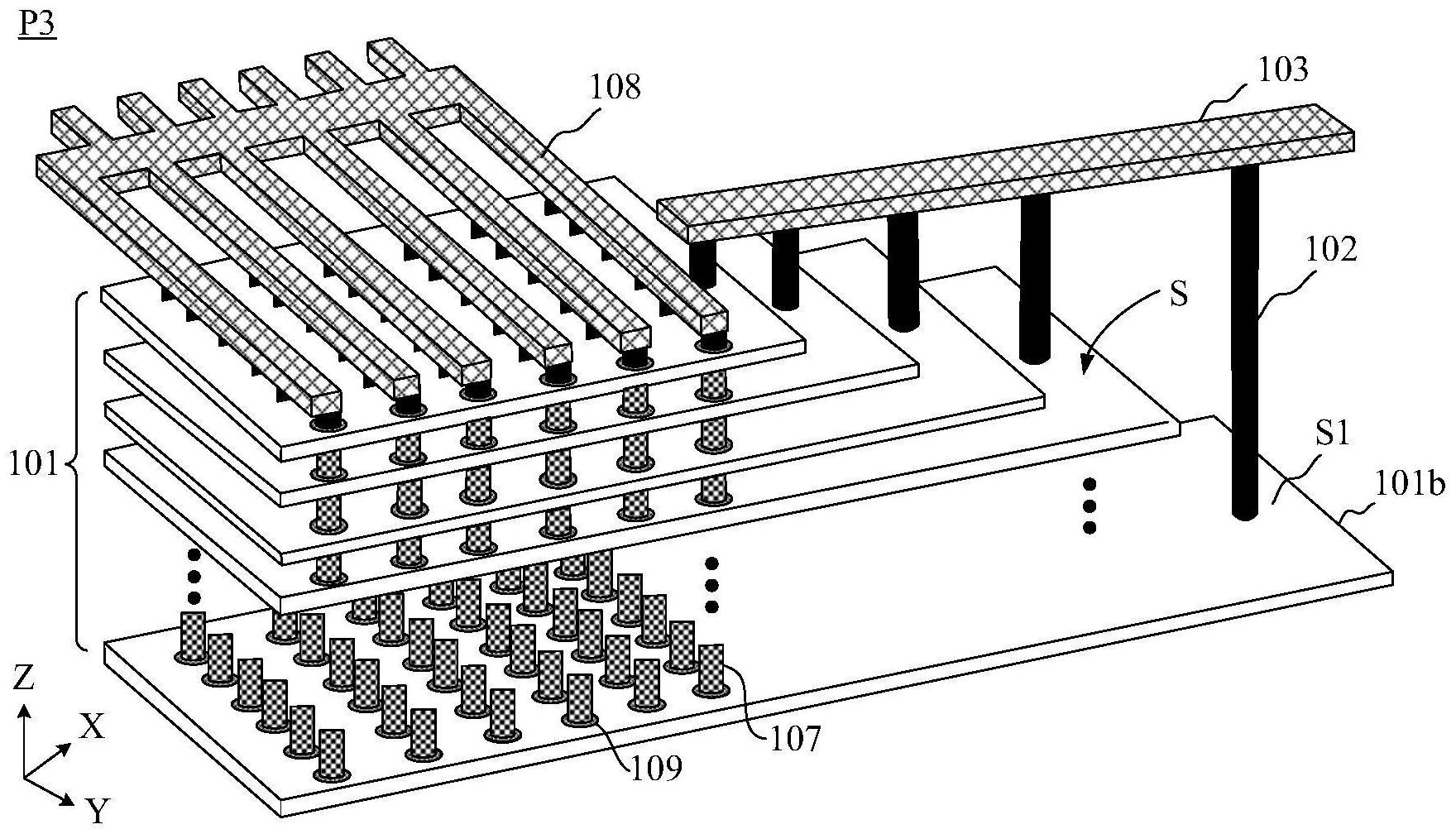
Huawei Technologies Co., Ltd. has recently added several pieces of patent information, one of which is titled "Semiconductor Structure and Preparation Methods, 3D memory, and Electronic Equipment" with the public number CN116940110A..


Image

Image

Image
 
Status
Not open for further replies.
Top