You are using an out of date browser. It may not display this or other websites correctly.
You should upgrade or use an alternative browser.
You should upgrade or use an alternative browser.
Chinese semiconductor industry
- Thread starter Hendrik_2000
- Start date
- Status
- Not open for further replies.
alright, I have to revert myself. Looks like there was a beijing 汉天下 that got renamed to OnMicro and there is also a suzhou 汉天下 that produces baw filters (website ). OnMicro also produces L-PAMiD modulesAlright on 昂瑞微 (OnMicro), formerly known as 汉天下(Huntersun)
By 2021, it had sold over 100m BAW filter
So, back to square 1 in figuring out which company is supply BAW filters
this on china's rf supply chain.
most common and highest market share is in switches and LNA
followed by PAs射频开关和LNA是国产化率较高的射频前端器件。国内有开关和LNA产品的厂商很多,如卓胜微、紫光展锐、昂瑞微、艾为电子、飞骧科技、唯捷创芯等,但把开关作为主要产品的公司较少,如卓胜微、韦尔股份、艾为电子
国内PA厂商众多,例如唯捷创芯、飞骧科技、紫光展锐、昂瑞微、慧智微、芯百特、芯朴科技、卓胜微等。目前以2G/3G/4G PA为主,市场竞争激烈,普遍盈利能力较差。不过,近两年国产公司正在向高价值的5G PA及模组进军,卓胜微、唯捷创芯、飞骧科技、芯朴科技、慧智微等公司目前已具备5G模组生产能力。
followed by SAW
Apparently, quite a few SAW suppliers. Maxscend is a major one but they also have shenzhen micro and a lot of other onesSAW滤波器市场主要的新进入者是国内厂商,国内SAW滤波器企业较多,但技术差距不大、收入体量较小,主要生产低端产品。相关企业包括卓胜微、德清华莹、好达电子、麦捷科技等。
and finally BAW
they mentioned memsonics, epicmem and Rofs Micro here. Not sure which other ones.BAW滤波器壁垒最高,工艺流程比SAW滤波器更加复杂,而且海外龙头Broadcom、Qorvo等进行了完善的专利布局,突破难度极大,中国厂商的市场份额约等于0。目前武汉敏芯、开元通信、天津诺思等厂商正在积极布局BAW。
If we accept the rather optimistic premise that a euv prototype has been assembled & testing will take 3 yrs but trial process with it can start low rate production in 2 years, that still leaves plenty of time for improvement in current smic process. I think n5 seems too hard at acceptable yield level based on what hvpc said, but no reason they can't improve density more & shrink features further like what Intel has done. If you can't achieve 15% gain in density for n+3, then try 5% or 10% every year.
Also, I wonder when hlmc can get started with 14nm production. They should have the tools to do it already. That will allow smic to shift more production to 7nm without hampering 14nm supplies.
I have seem some few techniques in the research literature that if sucessful could extent immersion beyond 7nm or even lower without EUV.If we accept the rather optimistic premise that a euv prototype has been assembled & testing will take 3 yrs but trial process with it can start low rate production in 2 years, that still leaves plenty of time for improvement in current smic process. I think n5 seems too hard at acceptable yield level based on what hvpc said, but no reason they can't improve density more & shrink features further like what Intel has done. If you can't achieve 15% gain in density for n+3, then try 5% or 10% every year.
Also, I wonder when hlmc can get started with 14nm production. They should have the tools to do it already. That will allow smic to shift more production to 7nm without hampering 14nm supplies.
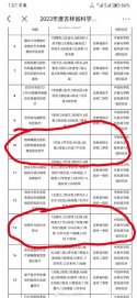
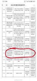
someone posted online of this summarizing the various awards related to EUV project that has been publicized recently
I haven't checked to verify that all of these in fact have happened, but there is certainly a lot of news and rumors on it recently


well, this seems to be posted somewhere on website for people to take screen shot of this
3 awards for EUV project it looks like for different part. Of which 1 was top level award from Jilin province to CAS & CIOMP
the other 2 are 2nd level award
10 translates to Ultra-high-precision lithography machine imaging objective lens system wave aberration detection technology
13 translates to EUV lithography light technology
16 translates to EUV lithography multi-layer surface pollution prevention and non-destructive cleaning technology
This is on top of all the patents we have seen.
Now, let's hope Huawei with all its highly paid researchers can help SMIC & CAS/CIOMP/SIOM get this integrated and tested sooner rather than later.
Exactly, if anything the industry chases advanced nodes because it lets them be more slack, even lazy, on these other aspects of circuit optimization. This bottleneck will end up proving a great boon for Chinese semiconductors design ultimately because it’s forcing Chinese industry to get good at the things everyone else will eventually need to get good at if they want to compete once the shrinking game has been *completely* exhausted.YES.
Circuit performance can be improved by “critical path optimization” at the physical design level.
Critical path optimization steps:
First design > circuit extraction > SPICE simulation > transistor re-sizing > circuit extraction > SPICE simulation > transistor re-sizing > … repeating
----------
Circuit performance can also be improved by human intervention at floor planning, placement, and routing level.
----------
Performance can also be improved by developing more efficient signal processing methods.
There are many possibilities other than using better Xnm node.
Very good engineers are needed to do the above.
we first had people shrink NAND until it can't shrink anymore (SMIC still at 24nm for SLC Nand) and then started going 3DExactly, if anything the industry chases advanced nodes because it lets them be more slack, even lazy, on these other aspects of circuit optimization. This bottleneck will end up proving a great boon for Chinese semiconductors design ultimately because it’s forcing Chinese industry to get good at the things everyone else will eventually need to get good at if they want to compete once the shrinking game has been *completely* exhausted.
DRAM is shrinking right now and will hit limit at 10nm and then start to go 3D. Since Chinese DRAM players don't have EUV at the moment, they are going to try 3D DRAM earlier as Huawei's patents show
At some point, we reach a point of diminishing return with logic nodes also. SRAM already can't shrink and are occupying larger and larger % of the die. and then we have the dark matter issue which gets worse as features shrink.
So we will probably have to go to 3D logic once that happens. If HW is temporarily slowed down by lack of EUV, it will just have to do more 3D stacking.
That's why I was encouraged with the lack of stacking in Kirin 9000S. They can still pack in more transistors without increasing die size later by stacking. power consumption probably won't be great, but if they can get power consumption under control in other places like RF and increase battery densities, I don't see why people would care.
Now I clearly don't work in chip designs, so I don't quite know how much more optimized HW can get with Kirin chips using current SMIC process. I assume they haven't exhausted those areas yet. I would say that as yield improve & they can do larger die, that may also give them more options. Obviously, further shrinking by SMIC also helps
This is by no means groundbreaking, I'm afraid. According to Apple, iPhones going back to the iPhone 7 can survive water immersion to certain depths for up to 30 minutes:
When they said the phone is waterproof I thought they meant it will function if you spilled drinks on it, not that you can submerge the whole thing while it is still on!
iPhone 12-14 => 6 meters
iPhone 11 Pro => 4 meters
iPhone 11, XS => 2 meters
iPhone SE (2nd generation), XR, X, 8, 7 => 1 meter
- Status
- Not open for further replies.


