Correction - Hisilicon developing Multi Patterning process for production of 12nm Chips.@WTAN , We had discuss this before but I need your clarification , will SMIC supply HW with its N+1 to be produced this April or even its 14nm? I got conflicting reports saying otherwise.
You are using an out of date browser. It may not display this or other websites correctly.
You should upgrade or use an alternative browser.
You should upgrade or use an alternative browser.
Chinese semiconductor industry
- Thread starter Hendrik_2000
- Start date
- Status
- Not open for further replies.
@WTAN Thanks for the info, @localizer I read that news as well, their savior is the SMIC N+2 , but is good only for the mid range phone, a big IF SMIC is able to mass produced it this year. So Its the end of the line for the P and Mate series of phone , its sad I'm really looking forward of replacing my P30 PRO with a P50 PRO, well I think I'll have to wait until 2024, with the current economic situation, It gave me a reason to wait.From what I’ve read on Chinese media they’re giving up on the 14nm kirin 710a due to poor performancez
They should dedicate all 14nm chips to base stations and IOT.
Phones they will have to wait probably.
I believe SMIC is quietly supplying Huawei 14nm Chips. Huawei recently launched a new budget Smartphone using a new model 14nm SOC.
As for the N+1, it depends on the progress of SMIC in developing its new De-Americanised FAB.
If progress if smooth and SMIC is confident it can run its FAB without much American input, then it will eventually supply Huawei.
But time is running out for SMIC to supply Huawei as Huawei will very soon have its own
De-Americanised FAB.
Huawei will work with its partner ICRD to eventually produce its own 7nm Chips.
I noticed in the Workshop on FAB Tech posted above that Hisilicon is designing 12nm FINFET Chips.
These are likely SMIC chips Huawei stockpiled prior to the sanctions kicking in.
Even recently Huawei anounced a smartphone with 5nm TSMC manufactured chips. SMIC was sanctioned way after TSMC.
You can't just stop a production line once you get a notification. Fabbing a chip from start to finish takes a long time and you typically don't interrupt production before the chips exit the production line. If production is stopped midway, like during an earthquake, it can be really hard to restart. Plus you are throwing a lot of money down the drain.
The 710A used might be the Chips Huawei stockpiled, but with the new Chinese Entity List Laws and the new Biden Admin, it is also likely that SMIC would have taken the opportunity to quietly resume supply of 14nm Chips to Huawei.These are likely SMIC chips Huawei stockpiled prior to the sanctions kicking in.
Even recently Huawei anounced a smartphone with 5nm TSMC manufactured chips. SMIC was sanctioned way after TSMC.
You can't just stop a production line once you get a notification. Fabbing a chip from start to finish takes a long time and you typically don't interrupt production before the chips exit the production line. If production is stopped midway, like during an earthquake, it can be really hard to restart. Plus you are throwing a lot of money down the drain.
SMIC is only prevented by the US from producing 10nm Chips or under.
In any case Huawei would probably be producing its own 12nm or 14nm Chips in 2022.
Since medium and low ended phone brand honor got sold. Huawei doesn't have a need for Kirin 710a for phone .From what I’ve read on Chinese media they’re giving up on the 14nm kirin 710a due to poor performancez
They should dedicate all 14nm chips to base stations and IOT.
Phones they will have to wait probably.
Kirin710a is for car.
@WTAN If that is the case, HW will not avail the SMIC N+1 (8nm) this April?The 710A used might be the Chips Huawei stockpiled, but with the new Chinese Entity List Laws and the new Biden Admin, it is also likely that SMIC would have taken the opportunity to quietly resume supply of 14nm Chips to Huawei.
SMIC is only prevented by the US from producing 10nm Chips or under.
In any case Huawei would probably be producing its own 12nm or 14nm Chips in 2022.
The SMIC N+1 is under 10nm so it is a bit trickier.@WTAN If that is the case, HW will not avail the SMIC N+1 (8nm) this April?
SMIC has to take into account the new Chinese Entity List Laws, the US response as well as losing revenue from Huawei.
We will just have to wait till later in the year to find out.
But one thing for certain is that Huawei will eventually produce its own 7nm Chips.
This is in 2018, EUV photoresist project
=============================================================================
2018-05-30
5月24日,国家科技重大专项“极大规模集成电路制造装备及成套工艺”专项(以下简称02重大专项)实施管理办公室组织任务验收专家组、财务验收专家组对02重大专项“极紫外光刻胶材料与实验室检测技术研究”项目进行了任务验收和财务验收。与会专家听取了项目负责人和课题负责人对项目和课题完成情况的汇报、测试组的现场测试报告、财务执行情况报告等,审阅了验收资料。经过认真讨论,与会专家一致同意该项目通过验收。
极大规模集成电路制造装备与成套工艺”专项(02专项)项目“极紫外光刻胶材料与实验室检测技术研究”由中国科学院化学研究所、中国科学院理化技术研究所、北京科华微电子材料有限公司联合承担。经过项目组全体成员的努力攻关,完成了EUV光刻胶关键材料的设计、制备和合成工艺研究、配方组成和光刻胶制备、实验室光刻胶性能的初步评价装备的研发,达到了任务书中规定的材料和装备的考核指标。项目共申请发明专利15项(包括国际专利5项),截止到目前,共获得授权专利10项(包括国际专利授权3项);培养了博士研究生9名,硕士研究生1名。
On May 24, the National Science and Technology Major Special Project "Very Large Scale Integrated Circuit Manufacturing Equipment and Complete Processes" (hereinafter referred to as the 02 Major Project) Implementation Management Office organized the task acceptance expert group and the financial acceptance expert group on the 02 major special project "Extreme Ultraviolet Light". Task acceptance and financial acceptance were carried out for the project "Research on Resist Materials and Laboratory Testing Technology". The participating experts listened to the reports of the project leader and the subject leader on the completion of the project and the subject, the field test report of the test team, the financial performance report, etc., and reviewed the acceptance materials. After serious discussion, the participating experts agreed that the project passed the acceptance.
The special project of "Extremely large-scale integrated circuit manufacturing equipment and complete technology" (02 special) project "Extreme ultraviolet photoresist materials and laboratory testing technology research" is sponsored by Institute of Chemistry, Chinese Academy of Sciences, Institute of Physics and Chemistry, Chinese Academy of Sciences, Beijing Kehua Jointly undertaken by Materials Co., Ltd. After the hard work of all members of the project team, the design, preparation and synthesis process research of EUV photoresist key materials, formula composition and photoresist preparation, and preliminary evaluation equipment for laboratory photoresist performance have been completed The research and development of the company has reached the assessment indicators of materials and equipment specified in the mission statement. The project has applied for 15 invention patents (including 5 international patents), and so far, a total of 10 authorized patents have been obtained (including 3 international patents) ; Trained 9 doctoral students and 1 master student.

This is the first generation of EUV system developed. It started 2009 and completed in 2017. Its resolution is about 32nm.
They do have some back ground on this. Its not like they doing EUV from scratch now.
They could really speed it up if companies like Huawei, ZTE, SMIC sponsoring them and adopting the system in the industry a while back, before they got hit by sanctions. Maybe have to thank Trump otherwise all their research is just research , stashed in the lab.
====================================================================
2017-07-12
Recently, the National Science and Technology Major Project (02 Project) Implementation Management Office of "Very Large Scale Integrated Circuit Manufacturing Equipment and Complete Processes" organized experts to hold the "Extreme Ultraviolet Lithography Key Technology Research" project at the Changchun Institute of Optics, Fine Mechanics and Physics, Chinese Academy of Sciences At the acceptance meeting, the Institute of Optoelectronics undertook the seventh topic of the project "Development of experimental equipment and vacuum system for the principle of extreme ultraviolet lithography." The evaluation expert group fully affirmed the series of results achieved by the project, unanimously agreed that the project passed the acceptance, and believed that the research work of the project provided strong support for the smooth implementation of the entire project, and accumulated the core technical foundation for the further development of extreme ultraviolet lithography.
Extreme Ultraviolet (EUV) lithography is a projection lithography technology that uses 13.5nm as the exposure light source, and is recognized as the most promising next-generation lithography technology. "Research on Key Technologies of Extreme Ultraviolet Lithography" is a forward-looking research project aimed at breaking through the foreign technology blockade in the development of extreme ultraviolet lithography. The subject of "Experimental Device Machinery and Vacuum System Development for Extreme Ultraviolet Lithography Principles" undertaken by Optoelectronics is one of the important research contents of the project, which mainly solves the high-stability vacuum environment of the exposure device, active vibration reduction, automatic film transport system, and high-precision workpieces. Key technologies such as stage control and nanometer leveling and focusing measurement system are indispensable components for the integration and testing of extreme ultraviolet lithography exposure equipment. The system to be developed for this subject is complex, with many development contents and technical difficulties.
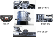
After eight years of hard work, the team of the General Research Laboratory of Microelectronics Equipment of the Institute of Optoelectronics has broken through key unit technologies such as vacuum, film transport, work table, vibration reduction and coke detection: the vacuum system achieves a stable high vacuum environment of 5.8×10⁻⁷ Torr, which ensures The stability of EUV light source propagation; the whole frame and damping system meet the VC-F damping standard, the horizontal direction 2.2Hz-500Hz, the vertical direction 2Hz-500Hz frequency range has good vibration isolation effect, and the frame, workpiece table and mask table are stable The performance meets the requirements of 32nm lithography and sub-nanometer wave aberration detection; the leveling and focusing detection system achieves nanometer level detection accuracy, which provides a guarantee for the continuous reproduction of 32nm lithography resolution. At the same time, in the development of the workpiece stage, the collaborative control technology of multiple workpiece stages was researched on the existing basis, which solved the simultaneous control and position switching problems of the silicon wafer stage and the image table, the mask stage and the object stage; automatic film transport system Realize fully automatic loading and unloading of films in a vacuum environment; the software system completes multi-module complex control, and coordinates various sub-systems to complete the exposure process.
On the basis of completing the development of the key unit system, cooperated with the overall project unit Changchun Institute of Optics and Mechanics to achieve 32nm repeatable exposure and cooperated with Shanghai Institute of Optics and Mechanics to achieve sub-nanometer wave aberration detection has played a major role. And the acceptance group experts praised. During the research and development of the project, the research team has made a series of original achievements in the fields of workpiece table control and precision measurement technology, and has applied for 31 invention patents, including 28 domestic patents and 3 international patents.
The successful acceptance of the subject indicates that the overall research team of the Microelectronics Equipment of the Institute of Optoelectronics has become an important part of the extreme ultraviolet lithography research team in my country. At the same time, it also shows that my country has broken through the core technology of EUV lithography equipment research and development, laying a solid technical foundation for the next development of EUV lithography.


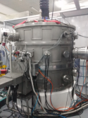
装置总体及关键单元系统 装置实物
They do have some back ground on this. Its not like they doing EUV from scratch now.
They could really speed it up if companies like Huawei, ZTE, SMIC sponsoring them and adopting the system in the industry a while back, before they got hit by sanctions. Maybe have to thank Trump otherwise all their research is just research , stashed in the lab.
====================================================================
2017-07-12
Recently, the National Science and Technology Major Project (02 Project) Implementation Management Office of "Very Large Scale Integrated Circuit Manufacturing Equipment and Complete Processes" organized experts to hold the "Extreme Ultraviolet Lithography Key Technology Research" project at the Changchun Institute of Optics, Fine Mechanics and Physics, Chinese Academy of Sciences At the acceptance meeting, the Institute of Optoelectronics undertook the seventh topic of the project "Development of experimental equipment and vacuum system for the principle of extreme ultraviolet lithography." The evaluation expert group fully affirmed the series of results achieved by the project, unanimously agreed that the project passed the acceptance, and believed that the research work of the project provided strong support for the smooth implementation of the entire project, and accumulated the core technical foundation for the further development of extreme ultraviolet lithography.
Extreme Ultraviolet (EUV) lithography is a projection lithography technology that uses 13.5nm as the exposure light source, and is recognized as the most promising next-generation lithography technology. "Research on Key Technologies of Extreme Ultraviolet Lithography" is a forward-looking research project aimed at breaking through the foreign technology blockade in the development of extreme ultraviolet lithography. The subject of "Experimental Device Machinery and Vacuum System Development for Extreme Ultraviolet Lithography Principles" undertaken by Optoelectronics is one of the important research contents of the project, which mainly solves the high-stability vacuum environment of the exposure device, active vibration reduction, automatic film transport system, and high-precision workpieces. Key technologies such as stage control and nanometer leveling and focusing measurement system are indispensable components for the integration and testing of extreme ultraviolet lithography exposure equipment. The system to be developed for this subject is complex, with many development contents and technical difficulties.
After eight years of hard work, the team of the General Research Laboratory of Microelectronics Equipment of the Institute of Optoelectronics has broken through key unit technologies such as vacuum, film transport, work table, vibration reduction and coke detection: the vacuum system achieves a stable high vacuum environment of 5.8×10⁻⁷ Torr, which ensures The stability of EUV light source propagation; the whole frame and damping system meet the VC-F damping standard, the horizontal direction 2.2Hz-500Hz, the vertical direction 2Hz-500Hz frequency range has good vibration isolation effect, and the frame, workpiece table and mask table are stable The performance meets the requirements of 32nm lithography and sub-nanometer wave aberration detection; the leveling and focusing detection system achieves nanometer level detection accuracy, which provides a guarantee for the continuous reproduction of 32nm lithography resolution. At the same time, in the development of the workpiece stage, the collaborative control technology of multiple workpiece stages was researched on the existing basis, which solved the simultaneous control and position switching problems of the silicon wafer stage and the image table, the mask stage and the object stage; automatic film transport system Realize fully automatic loading and unloading of films in a vacuum environment; the software system completes multi-module complex control, and coordinates various sub-systems to complete the exposure process.
On the basis of completing the development of the key unit system, cooperated with the overall project unit Changchun Institute of Optics and Mechanics to achieve 32nm repeatable exposure and cooperated with Shanghai Institute of Optics and Mechanics to achieve sub-nanometer wave aberration detection has played a major role. And the acceptance group experts praised. During the research and development of the project, the research team has made a series of original achievements in the fields of workpiece table control and precision measurement technology, and has applied for 31 invention patents, including 28 domestic patents and 3 international patents.
The successful acceptance of the subject indicates that the overall research team of the Microelectronics Equipment of the Institute of Optoelectronics has become an important part of the extreme ultraviolet lithography research team in my country. At the same time, it also shows that my country has broken through the core technology of EUV lithography equipment research and development, laying a solid technical foundation for the next development of EUV lithography.


装置总体及关键单元系统 装置实物
光电所承担的国家02专项项目“极紫外光刻关键技术研究”课题顺利通过验收 |
作者:四室 何渝 发布时间:2017-07-12 阅读次数: |
| 近日,“极大规模集成电路制造装备及成套工艺”国家科技重大专项(02专项)实施管理办公室组织专家在中国科学院长春光学精密机械与物理研究所召开了“极紫外光刻关键技术研究”项目验收会,光电所承担了该项目中的课题七“极紫外光刻原理实验装置机械与真空系统研制”。评审专家组充分肯定了课题取得的一系列成果,一致同意课题通过验收,认为该课题的研究工作为整个项目的顺利实施提供了有力支撑,为极紫外光刻的进一步发展积累了核心技术基础。 极紫外(Extreme Ultraviolet,EUV)光刻是以13.5nm为曝光光源的投影光刻技术,被公认为是最具潜力的下一代光刻技术。“极紫外光刻关键技术研究”作为一项前瞻性研究项目,旨在突破极紫外光刻研制中的国外技术封锁。光电所承担的“极紫外光刻原理实验装置机械与真空系统研制”课题为该项目的重要研究内容之一,主要解决曝光装置高稳定真空环境、主动减振、自动输片系统、高精度工件台控制和纳米级调平调焦测量系统等关键技术,是极紫外光刻曝光装置集成和试验必不可少的组成部分,该课题需研制的系统复杂、研制内容多、技术难度大。 光电所微电子装备总体研究室团队经过八年艰苦奋战,突破真空、输片、工件台、减振和检焦等关键单元技术:真空系统实现5.8×10⁻⁷Torr稳定的高真空环境,保证了EUV光源传播的稳定性;整机框架及减振系统达到VC-F减振标准,水平方向2.2Hz-500Hz、垂直方向2Hz-500Hz频率范围隔振效果良好,框架、工件台及掩模台稳定性满足32nm光刻需求和亚纳米级波像差检测;调平调焦检测系统实现了纳米级检测精度,为32nm光刻分辨力的连续多次复现提供了保障。同时,工件台研制中,在已有基础上研究了多工件台协同控制技术,解决了硅片台与像方台、掩模台与物方台的同时控制和位置切换问题;自动输片系统实现真空环境中的全自动上下片;软件系统完成多模块复杂控制,协调各分系统完成曝光流程。 在完成关键单元系统研制的基础上,配合项目总体单位长春光机所实现32nm可重复曝光以及配合上海光机所实现亚纳米波像差检测发挥了较大作用,受到项目总体单位、各课题单位及验收组专家好评。在课题的研制过程中,课题组在工件台控制、精密测量技术等领域取得了一系列原创性成果,累计申请发明专利31项,其中国内专利28项,国际专利3项。 课题顺利通过验收,表明光电所微电子装备总体研究室团队已经成为我国极紫外光刻研究队伍的重要组成部分。同时,也表明我国现已突破EUV光刻设备研发的核心技术,为EUV光刻的下一步发展奠定了坚实的技术基础。 |
Last edited:
- Status
- Not open for further replies.
