Chinese semiconductor industry

Status
Not open for further replies.

tonyget

Senior Member
Registered Member
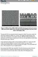
Gate pitch栅间距比其他厂的7nm工艺更宽松。然而相比去年的smic n+1工艺依然有所微缩。这说明n+2的单管密度仍然弱于其他厂的7nm。

然而通过其他的设计-生产协同优化(DTCO)。例如单扩散隔断(SDB),弥补了单管密度上的差距(和去年n+1的报告1个说法,应该还是6track高密度库)

较低的金属层体现出和smic n+1类似的布线策略,但是更小的gate pitch使得n+2工艺更接近于其他厂的7nm节点。和去年相比,上面这些进步使得n+2节点的std cell的高度缩小5%,cell面积缩小了10%

k9000s上的最新工艺说明中国大陆的晶圆厂可以不依托EUV进军7nm节点

The gate patch CDs are somewhat relaxed compared to other 7nm process nodes, but still shrunk compared to SMICs N+1 version. This suggests the gate density is less versus other 7nm devices in the market. However, with other design-technology co-optimization (DTCO) features implemented on this die, like single diffusion break (SDB).the gate density gap is reduced.

Lower metal layers feature similar routing strategies to SMIC's N+1 version, but with smaller CDs bring this SMIC N+2 process closer to other 7nm nodes. These enhancerments enabled SMIC to shrink its standard cell height (-5%) and standard cell area (-10%) compared to its N+1 implementation.

Discovering a Kirin 9000s chip uting SMIC's 7nm (N+2) foundry process in the new Huawei Mate 60 Pro smartphone demonstrates the technical progress China's semiconductor industry has been able to make without EUV lithography tools.
蜂蜜浏览器_火狐截图_2023-09-05T09-53-53.848Z.jpg
 
Last edited:

tphuang

Lieutenant General
Staff member
Super Moderator
VIP Professional
Registered Member
2022, I posted on twitter... SMIC shared Finfet technology with Huawei... in may this year, they publicly announced the Huawei Finfet patent...

Yes Sir, I had been following and researching trying to connect the dot, since SMIC use ASML equipment for its advance processes and is susceptible for further sanction by the US why not share the IP and get some royalties while waiting for their domestic FAB to come online. We know that they have a prototype SSA800 for verification and there are a lot of news about some Chinese firm buying up second hand DUVi equipment. So the speculation that Huawei is able to FAB its own chip is possible as PXW come to mind. Its a win win for both SMIC and Huawei as both were able synergize their effort and continue to do more R&D.

And also there is a huge market for SMIC 7nm either N+1 or N+2, it can't supply all of them, rather than FAB it to TSMC and risk National Security, its better to spread it around as SMIC can FAB and seek new customer at the expense of TSMC.

Sorry, this is just nonsense. You need a whole set of equipment outside of lithography machines in order to do all the multi-patterning work required for 7nm process. All of which became unavailable as of October and PXW only started operation this year

And this is also something continually improving at SMIC. Without the engineers with years of experience on this, how is Huawei going to improve on this process?

And finally, I have sources that say SMIC produced this! Not just well known bloggers on weibo

please stop making things up

Gate pitch栅间距比其他厂的7nm工艺更宽松。然而相比去年的smic n+1工艺依然有所微缩。这说明n+2的单管密度仍然弱于其他厂的7nm。

然而通过其他的设计-生产协同优化(DTCO)。例如单扩散隔断(SDB),弥补了单管密度上的差距(和去年n+1的报告1个说法,应该还是6track高密度库)

较低的金属层体现出和smic n+1类似的布线策略,但是更小的gate pitch使得n+2工艺更接近于其他厂的7nm节点。和去年相比,上面这些进步使得n+2节点的std cell的高度缩小5%,cell面积缩小了10%

k9000s上的最新工艺说明中国大陆的晶圆厂可以不依托EUV进军7nm节点

The gate patch CDs are somewhat relaxed compared to other 7nm process nodes, but still shrunk compared to SMICs N+1 version. This suggests the gate density is less versus other 7nm devices in the market. However, with other design-technology co-optimization (DTCO) features implemented on this die, like single diffusion break (SDB).the gate density gap is reduced.

Lower metal layers feature similar routing strategies to SMIC's N+1 version, but with smaller CDs bring this SMIC N+2 process closer to other 7nm nodes. These enhancerments enabled SMIC to shrink its standard cell height (-5%) and standard cell area (-10%) compared to its N+1 implementation.

Discovering a Kirin 9000s chip uting SMIC's 7nm (N+2) foundry process in the new Huawei Mate 60 Pro smartphone demonstrates the technical progress China's semiconductor industry has been able to make without EUV lithography tools.

View attachment 118231

I'm not really sure which other 7nm process they are comparing this against to say it has wider gate pitch, since there are so many and there are obvious improvements from earliest N7 to N7+.

I maintain this is basically N7+ in density & other performance areas. The original N+1 process was dense enough to be comparable to be early gen 7nm. So they shrunk it further and performance has been comparable to N5 fabb'd SoC & it's still more relaxed vs other 7nm process?
 

latenlazy

Brigadier
I'm not really sure which other 7nm process they are comparing this against to say it has wider gate pitch, since there are so many and there are obvious improvements from earliest N7 to N7+.

I maintain this is basically N7+ in density & other performance areas. The original N+1 process was dense enough to be comparable to be early gen 7nm. So they shrunk it further and performance has been comparable to N5 fabb'd SoC & it's still more relaxed vs other 7nm process?
It’s possible that they relaxed gate pitch but looked to other dimensional features to get higher density. Difficult to know whether that was due to achievable gate pitch limitations or if there were other optimization decisions going on. Either way the results are nothing to sneeze at.
 

tphuang

Lieutenant General
Staff member
Super Moderator
VIP Professional
Registered Member
AMEC's progress on 3D NAND and DRAM. AMEC is about to achieve 90% coverage on 3D NAND,100% coverage on sub-20nm DRAM.

View attachment 118203
View attachment 118204
View attachment 118205
View attachment 118206
This is great news. Looks like dram tools are fully validated. Just need to restart delivery on them. Good news for cxmt and all the other players looking to do 3d dram. At least, they can expand without sanction fears.

As for 3d nand, I would assume that other domestic players are involved because it's been said several times now that they can resume expansion here.

I would caution everyone that like with smic, this is just all on paper still. Until they get all the machines in there and increase production, we still have no end product. And ramping up production is a huge part of this.

But with this level of progress, I think they should at least finally progress to 17nm dram at some point in not so distant future.

Absolutely huge news
 
Last edited:

ansy1968

Brigadier
Registered Member
Sorry, this is just nonsense. You need a whole set of equipment outside of lithography machines in order to do all the multi-patterning work required for 7nm process. All of which became unavailable as of October and PXW only started operation this year

And this is also something continually improving at SMIC. Without the engineers with years of experience on this, how is Huawei going to improve on this process?

And finally, I have sources that say SMIC produced this! Not just well known bloggers on weibo

please stop making things up
You and I have the same source we PM each other, BUT aside from him there are others who gave me info, so let's just wait rather than dismissed them outright. Like PLA watching sometimes you need a little bit of clue to draw a big picture, that what make this thread exciting.
 

staplez

New Member
Registered Member
You and I have the same source we PM each other, BUT aside from him there are others who gave me info, so let's just wait rather than dismissed them outright. Like PLA watching sometimes you need a little bit of clue to draw a big picture, that what make this thread exciting.
Yeah, I have to agree here. There's absolutely no doubt that SMIC was involved. However, that doesn't mean SMIC didn't work hand in glove to help Huawei create the PXW fab and have it produce 7nm chips.

So it's possible this fab was secretly creating kirin 9000s chips using domestic processes like SMEE lithography and filled with SMIC engineers until Huawei engineers could take over. Obviously, this fab didn't make all the chips, after all we are looking at 20 million being created. I'm just saying I wouldn't discount that they did it at Huawei's fabs too.
 

ansy1968

Brigadier
Registered Member
Yeah, I have to agree here. There's absolutely no doubt that SMIC was involved. However, that doesn't mean SMIC didn't work hand in glove to help Huawei create the PXW fab and have it produce 7nm chips.
Here I think ICRD had a hand in helping Huawei since they sign a cooperative agreement and not only with Huawei BUT with ASML as well. Since ICRD had a NXT 1980i provide by ASML for R&D as stated by the MOU, couple with news of the Chinese buying second hand ASML duvi we can connect the dot and draw a tentative conclusion, it maybe speculation on our part BUT the evidence are there to be proven.

Please, Log in or Register to view URLs content!


Nov 8, 2020 — The plant would reportedly be run by a partner, Shanghai IC R&D Center, a chip research company backed by the Shanghai Municipal government. The ...

Missing: operate ‎| Show results with:
Please, Log in or Register to view URLs content!

Please, Log in or Register to view URLs content!


Nov 2, 2020 — According to The Financial Times, two people with knowledge about the project said the chip plant would be run by Shanghai IC R&D Center (ICRD), ...

Missing: operate ‎| Show results with:
Please, Log in or Register to view URLs content!


(ICRD), a public research consortium dedicated to the advancement of the semiconductor industry in China, and leading chip-making equipment manufacturer ASML Holding NV (ASML) signed a Memorandum of Understanding (MoU) to set up a jointly-owned world-class training center in Shanghai.Jun 21, 2017

Please, Log in or Register to view URLs content!

Please, Log in or Register to view URLs content!

Please, Log in or Register to view URLs content!

Please, Log in or Register to view URLs content!


Please, Log in or Register to view URLs content!


Feedback

Please, Log in or Register to view URLs content!

Please, Log in or Register to view URLs content!

Please, Log in or Register to view URLs content!

Please, Log in or Register to view URLs content!


Jun 20, 2017 — ICRD AND ASML SIGN MOU TO ESTABLISH A TRAINING CENTER IN SHANGHAI Source text for Eikon: Further company coverage: (Gdynia Newsroom)
So it's possible this fab was secretly creating kirin 9000s chips using domestic processes like SMEE lithography and filled with SMIC engineers until Huawei engineers could take over. Obviously, this fab didn't make all the chips, after all we are looking at 20 million being created. I'm just saying I wouldn't discount that they did it at Huawei's fabs too.
Thanks bro, from what I'm seeing China want to recreate the dynamics that makes Apple, TSMC, ASML great. Their interaction is the reason for their dominance. Since Huawei, SMIC and SMEE are under sanction it is obvious that the three of them need to work together to survived, so a big thank you Uncle Sam.
 
Last edited:

hvpc

Junior Member
Registered Member
Yeah, I have to agree here. There's absolutely no doubt that SMIC was involved. However, that doesn't mean SMIC didn't work hand in glove to help Huawei create the PXW fab and have it produce 7nm chips.

So it's possible this fab was secretly creating kirin 9000s chips using domestic processes like SMEE lithography and filled with SMIC engineers until Huawei engineers could take over. Obviously, this fab didn't make all the chips, after all we are looking at 20 million being created. I'm just saying I wouldn't discount that they did it at Huawei's fabs too.
PXW did not have a HVM ready production line a few months ago, which is necessary to build the Kirin9000s chips. They don't even have any scanners in their fab at the moment.
 

tphuang

Lieutenant General
Staff member
Super Moderator
VIP Professional
Registered Member
You and I have the same source we PM each other, BUT aside from him there are others who gave me info, so let's just wait rather than dismissed them outright. Like PLA watching sometimes you need a little bit of clue to draw a big picture, that what make this thread exciting.
hard no on that one. We are not using the same source in this case. I can assure you of that

So please stop your crazy conjectures.

PXW did not have a HVM ready production line a few months ago, which is necessary to build the Kirin9000s chips. They don't even have any scanners in their fab at the moment.
any idea when the production might start? It was supposedly this year. and they also said Swaysure by Q1 of 2024. Is that even possible?
 

BoraTas

Major
Registered Member
ASML's CEO Peter Wennik is telling the truth again. He was against export controls from the start.

Please, Log in or Register to view URLs content!

"I'm concerned about the earnings power of the Netherlands and of Europe, that we're at risk of falling behind," Wennink said.

He noted that the United States dominates big software platforms while Asia is ahead in car battery technologies and China is spending heavily on technical research.

"Every bloc sees the challenges, but they will do it (invest in business-academic partnerships) no matter what," he said at the opening of the academic year at Eindhoven Technical University.


"How are we going to compete? We have to start working closer together, now."

The executive said that while politicians respond to incidental problems, and praised initiatives such as Europe's Chips Act, they "lack vision" and don't invest structurally enough in science, education and industry.
 
Status
Not open for further replies.
Top